


双线路驱动器 DUAL LINE DRIVERS
The SN55110A, SN75110A, and SN75112 dual line drivers have improved output current regulation with supply voltage and temperature variations. In addition, the higher current of the SN75112 27 mA allows data to be transmitted over longer lines. These drivers offer optimum performance when used with the SN55107A, SN75107A, and SN75108A line receivers.
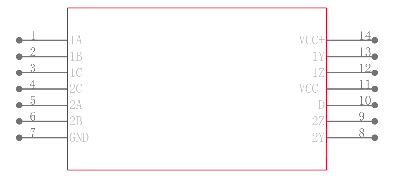
These drivers feature independent channels with common voltage supply and ground terminals. The significant difference between the three drivers is in the output-current specification. The driver circuits feature a constant output current that is switched to either of two output terminals by the appropriate logic levels at the input terminals. The output current can be switched off inhibited by low logic levels on the enable inputs. The output current is nominally 12 mA for the "110A devices, and is 27 mA for the SN75112.
The enable/inhibit feature is provided so the circuits can be used in party-line or data-bus applications. A strobe or inhibitor enable D, common to both drivers, is included for increased driver-logic versatility. The output current in the inhibited mode, IOoff, is specified so that minimum line loading is induced when the driver is used in a party-line system with other drivers. The output impedance of the driver in the inhibited mode is very high. The output impedance of a transistor is biased to cutoff.
The driver outputs have a common-mode voltage range of 3 V to 10 V, allowing common-mode voltage on the line without affecting driver performance.
All inputs are diode clamped and are designed to satisfy TTL-system requirements. The inputs are tested at 2 V for high-logic-level input conditions and 0.8 V for low-logic-level input conditions. These tests ensure 400-mV noise margin when interfaced with TTL Series 54/74.
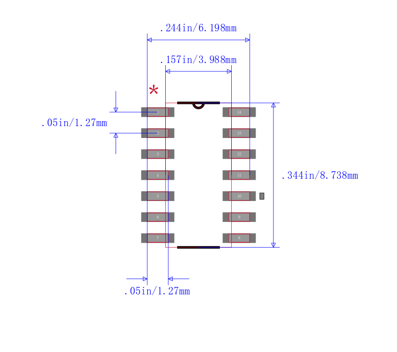
The SN55110A is characterized for operation over the full military temperature range of 55°C to 125°C. The SN75110A and SN75112 are characterized for operation from 0°C to 70°C.
| 型号/品牌 | 代替类型 | 替代型号对比 |
|---|---|---|
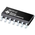
SN75112D TI 德州仪器 | 当前型号 | 当前型号 |
SN75112DR 德州仪器 | 完全替代 | SN75112D和SN75112DR的区别 |
SN75112DRE4 德州仪器 | 功能相似 | SN75112D和SN75112DRE4的区别 |