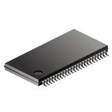
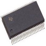

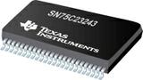
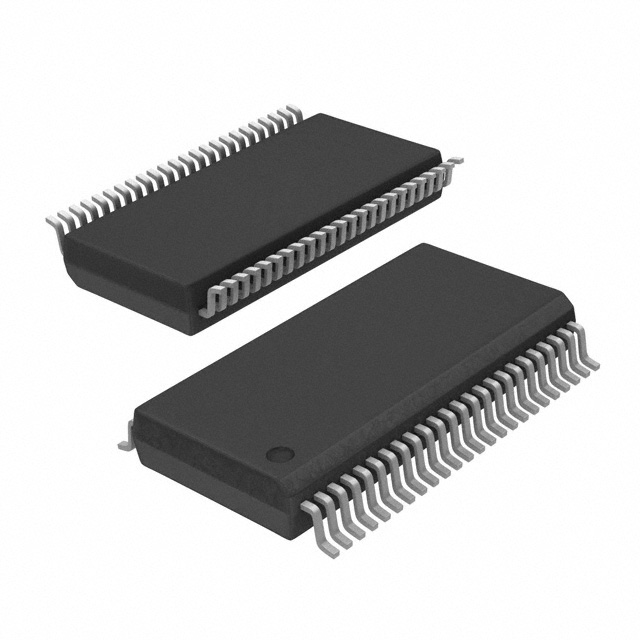
3 - V至5.5 V双RS - 232端口 3-V TO 5.5-V DUAL RS-232 PORT
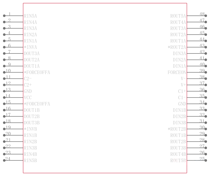
The SN65C23243 and SN75C23243 consist of two ports, each containing three line drivers and five line receivers, and a dual charge-pump circuit with ±15-kV ESD protection pin to pin serial-port connection pins, including GND. These devices meet the requirements of A/EIA-232-F and provide the electrical interface between an asynchronous communication controller and the serial-port connector. This combination of drivers and receivers matches that needed for two typical serial ports used in an IBM PC/AT, or compatible. The charge pump and four small external capacitors allow operation from a single 3-V to 5.5-V supply. In addition, these devices include an always-active noninverting output ROUT2\\\\ per port, which allows applications using the ring indicator to transmit data while the devices are powered down. The devices operate at data signaling rates up to 250 kbit/s, and a maximum of 30-V/µs driver output slew-rate.
Flexible control options for power management are available when either or both serial ports are inactive. The auto-powerdown feature functions when FORCEON is low and FORCEOFF\ is high. During this mode of operation, if the device does not sense a valid RS-232 signal, the driver outputs of its respective port are disabled. If FORCEOFF\ is set low, both drivers and receivers except ROUT2\\\\ are shut off, and the supply current is reduced to 1 µA. Disconnecting the serial port or turning off the peripheral drivers causes the auto-powerdown condition to occur.
Auto-powerdown can be disabled when FORCEON and FORCEOFF\ are high, and should be done when driving a serial mouse. With auto-powerdown enabled, the RS-232 port is activated automatically when a valid signal is applied to any respective receiver input. The INV\ output is used to notify the user if an RS-232 signal is present at any receiver input. INV\ is high valid data if any receiver input voltage is greater than 2.7 V or less than 2.7 V or has been between 0.3 V and 0.3 V for less than 30 µs. INV\ is low invalid data if all receiver input voltages are between 0.3 V and 0.3 V for more than 30 µs. Refer to Figure 5 for receiver input levels.
| 型号/品牌 | 代替类型 | 替代型号对比 |
|---|---|---|
SN75C23243DLR TI 德州仪器 | 当前型号 | 当前型号 |
SN65C23243DLR 德州仪器 | 完全替代 | SN75C23243DLR和SN65C23243DLR的区别 |
TRSF23243CDGGR 德州仪器 | 完全替代 | SN75C23243DLR和TRSF23243CDGGR的区别 |
SN75C23243DL 德州仪器 | 完全替代 | SN75C23243DLR和SN75C23243DL的区别 |