
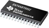

八进制挂号总线收发器扫描测试设备 SCAN TEST DEVICES WITH OCTAL REGISTERED BUS TRANSCEIVERS
The "ABT8952 scan test devices with octal registered bus transceivers are members of the Texas Instruments SCOPETM testability integrated-circuit family. This family of devices supports IEEE Standard 1149.1-1990 boundary scan to facilitate testing of complex circuit-board assemblies. Scan access to the test circuitry is accomplished via the 4-wire test access port TAP interface.
In the normal mode, these devices are functionally equivalent to the "BCT2952 and "ABT2952 octal registered bus transceivers. The test circuitry can be activated by the TAP to take snapshot samples of the data appearing at the device pins or to perform a self-test on the boundary-test cells. Activating the TAP in normal mode does not affect the functional operation of the SCOPETM octal registered bus transceivers.
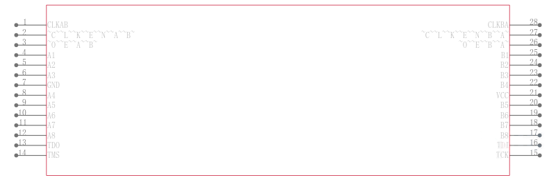
Data flow in each direction is controlled by clock CLKAB and CLKBA, clock-enable and , and output-enable and inputs. For A-to-B data flow, A-bus data is stored in the associated registers on the low-to-high transition of CLKAB, provided that is low. Otherwise, if is high or CLKAB remains at a static low or high level, the register contents are not changed. When is low, the B outputs are active. When is high, the B outputs are in the high-impedance state. Control for B-to-A data flow is similar to that for A-to-B, but uses CLKBA, , and .
In the test mode, the normal operation of the SCOPETM registered bus transceivers is inhibited, and the test circuitry is enabled to observe and control the I/O boundary of the device. When enabled, the test circuitry performs boundary-scan test operations as described in IEEE Standard 1149.1-1990.
Four dedicated test pins control the operation of the test circuitry: test data input TDI, test data output TDO, test mode select TMS, and test clock TCK. Additionally, the test circuitry performs other testing functions such as parallel signature analysis PSA on data inputs and pseudo-random pattern generation PRPG from data outputs. All testing and scan operations are synchronized to the TAP interface.
The SN54ABT8952 is characterized for operation over the full military temperature range of -55°C to 125°C. The SN74ABT8952 is characterized for operation from -40°C to 85°C.
电源电压DC 4.50V ~ 5.50V
输出接口数 8
电路数 8
位数 8
传送延迟时间 6.30 ns
电压波节 5.00 V
输出电流驱动 -500 µA
工作温度Max 85 ℃
工作温度Min -40 ℃
电源电压 4.5V ~ 5.5V
电源电压Max 5.5 V
电源电压Min 4.5 V
安装方式 Surface Mount
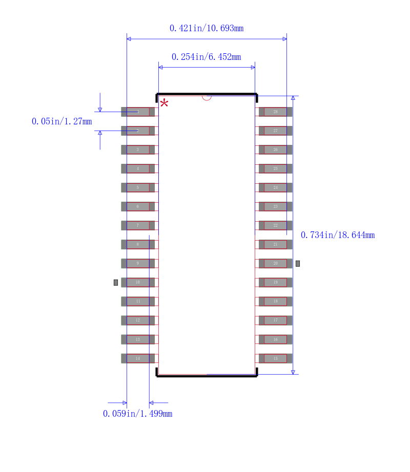
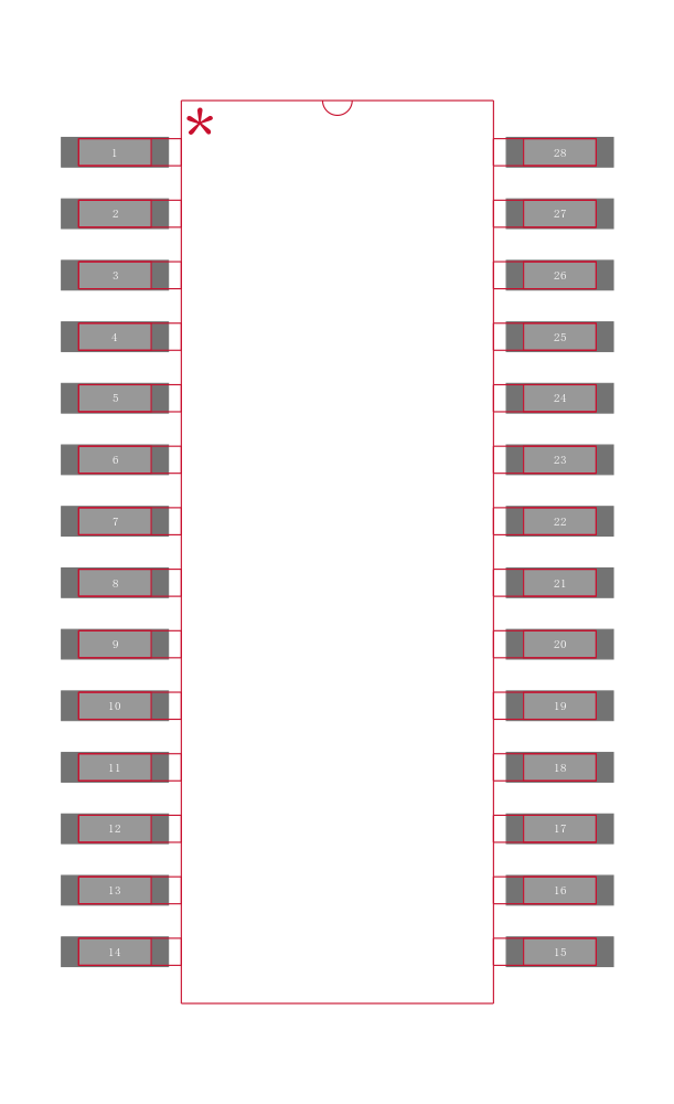
引脚数 28
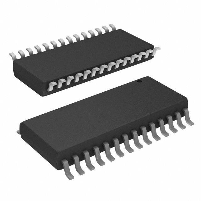
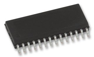
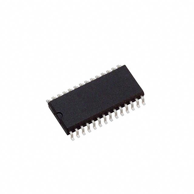
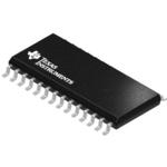
封装 SOIC-28
封装 SOIC-28
工作温度 -40℃ ~ 85℃
产品生命周期 Active
包装方式 Tube
RoHS标准 RoHS Compliant
含铅标准 Lead Free
REACH SVHC标准 No SVHC
REACH SVHC版本 2015/06/15
| 型号/品牌 | 代替类型 | 替代型号对比 |
|---|---|---|
SN74ABT8952DW TI 德州仪器 | 当前型号 | 当前型号 |
SN74ABT8952DWR 德州仪器 | 完全替代 | SN74ABT8952DW和SN74ABT8952DWR的区别 |
SN74ABT8952DWE4 德州仪器 | 完全替代 | SN74ABT8952DW和SN74ABT8952DWE4的区别 |
SN74ABT8952DWG4 德州仪器 | 完全替代 | SN74ABT8952DW和SN74ABT8952DWG4的区别 |