
具有预充电输出的5 V BUS开关8位FET总线开关-2 -V冲保护 8-BIT FET BUS SWITCH WITH PRECHARGED OUTPUTS 5-V BUS SWITCH WITH -2-V UNDERSHOOT PROTECTION
The SN74CBT6845C is a high-speed TTL-compatible FET bus switch with low ON-state resistance ron, allowing for minimal propagation delay. Active Undershoot-Protection Circuitry on the A and B ports of the SN74CBT6845C provides protection for undershoot up to 2 V by sensing an undershoot event and ensuring that the switch remains in the proper OFF state. The device also precharges the B port to a user-selectable bias voltage BIASV to minimize live-insertion noise.
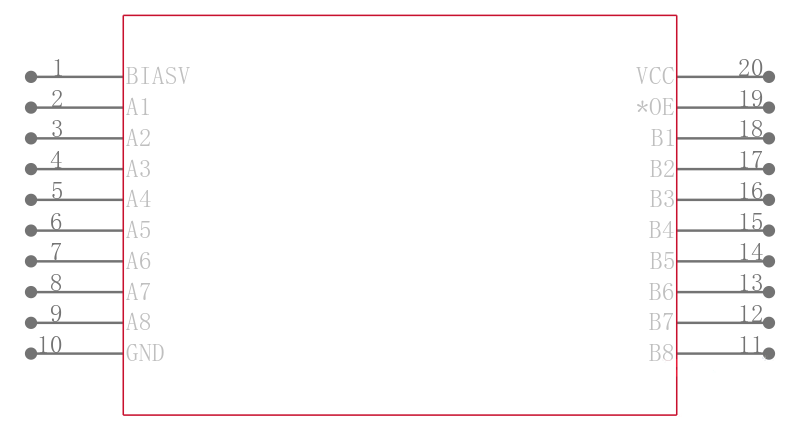
The SN74CBT6845C is an 8-bit bus switch with a single output-enable OE\\\\ input. When OE\ is low, the 8-bit bus switch is ON, and the A port is connected to the B port, allowing bidirectional data flow between ports. When OE\ is high, the 8-bit bus switch is OFF, and a high-impedance state exists between the A and B ports. The B port is precharged to BIASV through the equivalent of a 10-k resistor when OE\ is high, or if the device is powered down VCC = 0 V.
During insertion or removal of a card into or from an active bus, the cards output voltage may be close to GND. When the connector pins make contact, the cards parasitic capacitance tries to force the bus signal to GND, creating a possible glitch on the active bus. This glitching effect can be reduced by using a bus switch with precharged bias voltage BIASV of the bus switch equal to the input threshold voltage level of the receivers on the active bus. This method will ensure that any glitch produced by insertion or removal of the card will not cross the input threshold region of the receivers on the active bus, minimizing the effects of live-insertion noise.
This device is fully specified for partial-power-down applications using Ioff. The Ioff feature ensures that damaging current will not backflow through the device when it is powered down. The device has isolation during power off.
To ensure the high-impedance state during power up or power down, OE\ should be tied to VCC through a pullup resistor; the minimum value of the resistor is determined by the current-sinking capability of the driver.
| 型号/品牌 | 代替类型 | 替代型号对比 |
|---|---|---|
SN74CBT6845CDGVR TI 德州仪器 | 当前型号 | 当前型号 |
SN74CBT6845CPWR 德州仪器 | 完全替代 | SN74CBT6845CDGVR和SN74CBT6845CPWR的区别 |
SN74CBT6845CDGVRE4 德州仪器 | 完全替代 | SN74CBT6845CDGVR和SN74CBT6845CDGVRE4的区别 |
SN74CBT6845CPWG4 德州仪器 | 完全替代 | SN74CBT6845CDGVR和SN74CBT6845CPWG4的区别 |