


低功耗, 1.8 / 2.5 / 3.3 V输入, 3.3 V CMOS输出, 2输入正或门 LOW POWER, 1.8/2.5/3.3-V INPUT,3.3-V CMOS OUTPUT, 2-INPUT POSITIVE-OR GATE
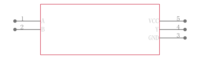
Y = A + B or Y = A B •
DESCRIPON/ORDERING INFORMATION
The SN74AUP1T32 performs the Boolean function with designation for logic-level translation applications with output referenced to supply VCC. AUP technology is the industry"s lowest-power logic technology designed for use in extending battery-life in operating. All input levels that accept 1.8-V LVCMOS signals, while operating from either a single 3.3-V or 2.5-V VCC supply. This product also maintains excellent signal integrity see Figure 1 and Figure 2.
FEATURES
• Single-Supply Voltage Translator
• Output Level Up to Supply VCC CMOS Level
– 1.8 V to 3.3 V at VCC= 3.3 V
– 2.5 V to 3.3 V at VCC= 3.3 V
– 1.8 V to 2.5 V at VCC= 2.5 V
– 3.3 V to 2.5 V at VCC= 2.5 V
• Schmitt-Trigger Inputs Reject Input Noise and Provide Better Output Signal Integrity
• Ioff Supports Partial Power Down VCC= 0 V
• Very Low Static Power Consumption: 0.1 µA
• Very Low Dynamic Power Consumption: 0.9 µA
• Latch-Up Performance Exceeds 100 mA Per JESD 78, Class II
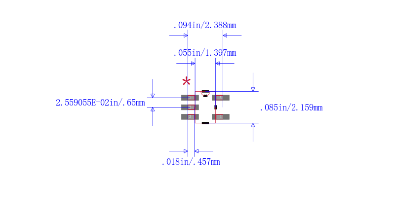
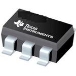
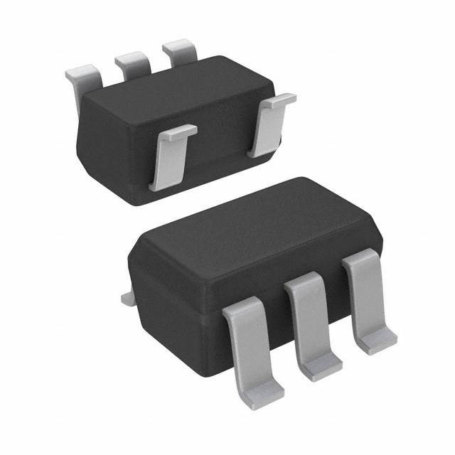
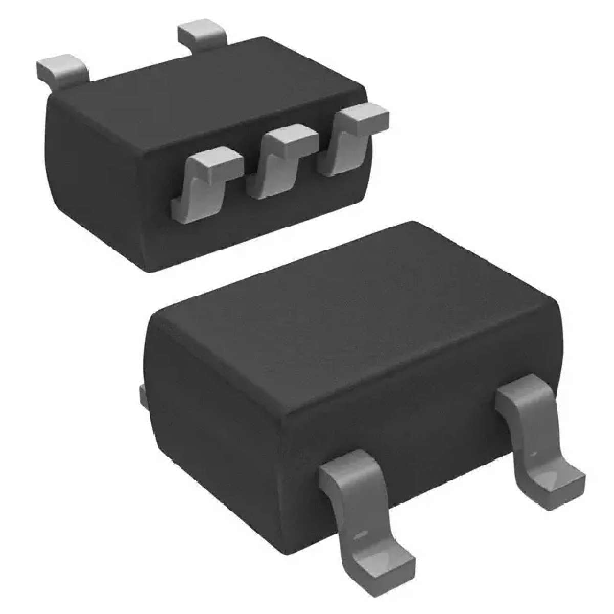
• Pb-Free Packages Available: SC-70 DCK 2 x 2.1 x 0.65 mm Height 1.1 mm
• More Gate Options Available at www.ti.com/littlelogic
• ESD Performance Tested Per JESD 22
– 2000-V Human-Body ModelA114-B, Class II
– 1000-V Charged-Device Model C101
输出接口数 1
输出电压 3.6 V
输出电流 4 mA
电路数 1
位数 1
传送延迟时间 10.0 ns
逻辑门个数 1
输入数 2
工作温度Max 85 ℃
工作温度Min -40 ℃
电源电压 2.3V ~ 3.6V
电源电压Max 3.6 V
电源电压Min 2.3 V
安装方式 Surface Mount
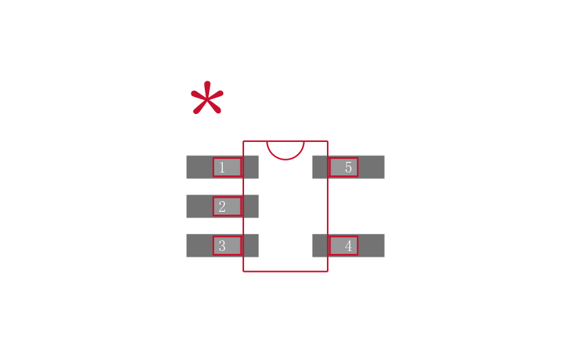
引脚数 5
封装 SC-70-5
高度 1 mm
封装 SC-70-5
工作温度 -40℃ ~ 85℃
产品生命周期 Active
包装方式 Tape & Reel TR
RoHS标准 RoHS Compliant
含铅标准 Lead Free
ECCN代码 EAR99