


单3输入正或与门 SINGLE 3-INPUT POSITIVE OR-AND GATE
DESCRIPON
This device is designed for 1.65-V to 5.5-V VCC operation.
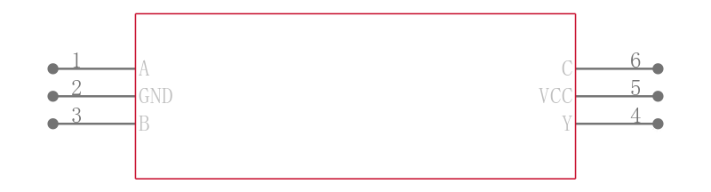
The SN74LVC1G3208 device is a single 3-input positive OR-AND gate. It performs the Boolean function Y = A + B ● C in positive logic. By tying one input to GND or VCC, the SN74LVC1G3208 device offers two more functions.
When C is tied to VCC, this device performs as a 2-input OR gate Y = A + B. When A is tied to GND, the device works as a 2-input AND gate Y = B ● C.
This B is tied device to GND also Y works = A ●asC. a 2-input AND gate when NanoStar™ and NanoFree™ package technology is a major breakthrough in IC packaging concepts, using the die as the package.
This device is fully specified for partial-power-down applications using Ioff. The Ioff circuitry disables the outputs, preventing damaging current backflow through the device when it is powered down.
FEATURES
• Available in the Texas Instruments NanoStar™ and NanoFree™ Packages
• Supports 5-V VCC Operation
• Inputs Accept Voltages to 5.5 V
• Provides Down Translation to VCC
• Max tpd of 5 ns at 3.3 V
• Low Power Consumption, 10-µA Max ICC
• ±24-mA Output Drive at 3.3 V
• Input Hysteresis Allows Slow Input Transition and Better Switching Noise Immunity at the Input Vhys = 250 mV Typ @ 3.3 V
• Can Be Used in Three Combinations:
– OR-AND Gate
– OR Gate
– AND Gate
• Ioff Supports Live Insertion, Partial-Power-Down Mode, and Back-Drive Protection
• Latch-Up Performance Exceeds 100 mA Per JESD 78, Class II
• ESD Protection Exceeds JESD 22
– 2000-V Human-Body Model A114-A
– 200-V Machine Model A115-A
– 1000-V Charged-Device Model C101
电源电压DC 1.65V ~ 5.50V
电路数 1
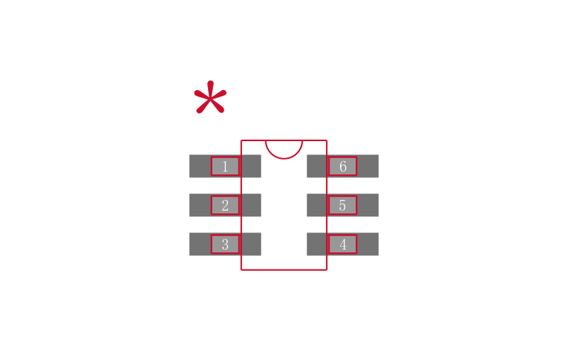
针脚数 6
位数 1
传送延迟时间 3.40 ns
电压波节 5.00 V, 3.30 V, 2.50 V, 1.80 V
逻辑门个数 1
输入数 3
工作温度Max 125 ℃
工作温度Min -40 ℃
电源电压 1.65V ~ 5.5V
电源电压Max 5.5 V
电源电压Min 1.65 V
安装方式 Surface Mount
引脚数 6
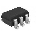
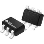
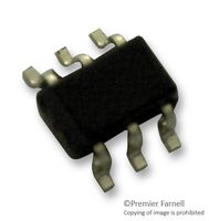
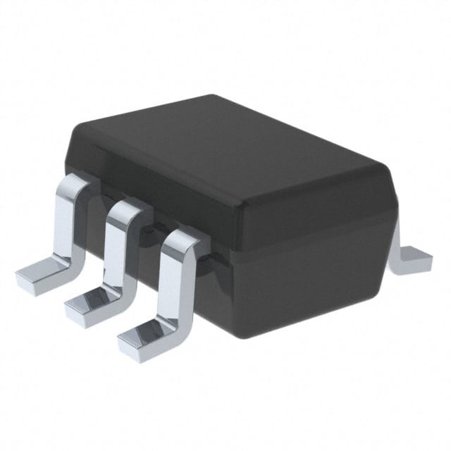
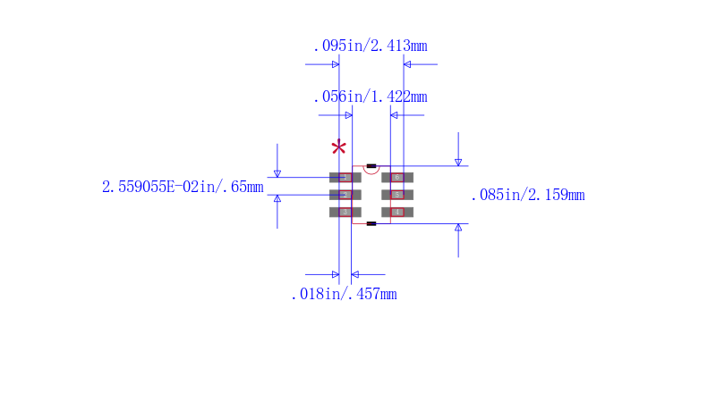
封装 SC-70-6
高度 1 mm
封装 SC-70-6
工作温度 -40℃ ~ 85℃
产品生命周期 Active
包装方式 Tape & Reel TR
RoHS标准 RoHS Compliant
含铅标准 Lead Free
ECCN代码 EAR99
| 型号/品牌 | 代替类型 | 替代型号对比 |
|---|---|---|
SN74LVC1G3208DCKR TI 德州仪器 | 当前型号 | 当前型号 |
74LVC1G3208DCKTE4 德州仪器 | 完全替代 | SN74LVC1G3208DCKR和74LVC1G3208DCKTE4的区别 |
74LVC1G3208DCKRE4 德州仪器 | 完全替代 | SN74LVC1G3208DCKR和74LVC1G3208DCKRE4的区别 |
74LVC1G3208DCKRG4 德州仪器 | 完全替代 | SN74LVC1G3208DCKR和74LVC1G3208DCKRG4的区别 |