低功耗可配置的多功能的门 LOW-POWER CONFIGURABLE MULTIPLE-FUNCTION GATE
The AUP family is s premier solution to the industrys low-power needs in battery-powered portable applications. This family ensures a very low static- and dynamic-power consumption across the entire VCC range of 0.8 V to 3.6 V, resulting in increased battery life see Figure 1. This product also maintains excellent signal integrity see the very low undershoot and overshoot characteristics shown in Figure 2.
The SN74AUP1G98 features configurable multiple functions. The output state is determined by eight patterns of 3-bit input. The user can choose the logic functions MUX, AND, OR, NAND, NOR, inverter, and noninverter. All inputs can be connected to VCC or GND.
The device functions as an independent gate with Schmitt-trigger inputs, which allow for slow input transition and better switching-noise immunity at the input.
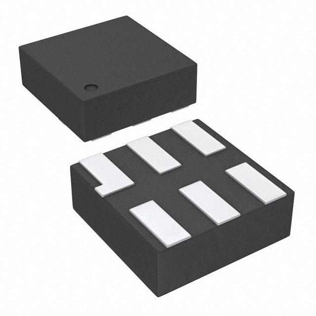
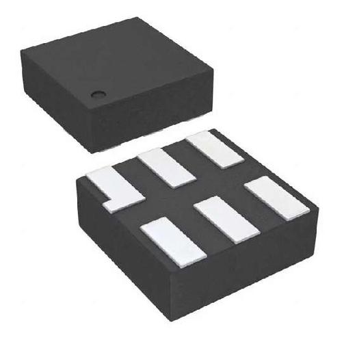
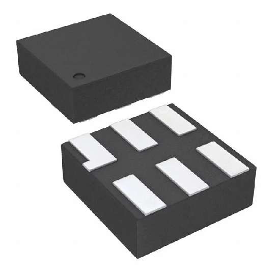
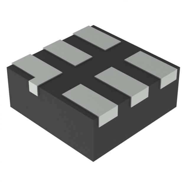
NanoStar™ package technology is a major breakthrough in IC packaging concepts, using the die as the package.
This device is fully specified for partial-power-down applications using Ioff. The Ioff circuitry disables the outputs, preventing damaging current backflow through the device when it is powered down.
电源电压DC 800mV ~ 3.60V
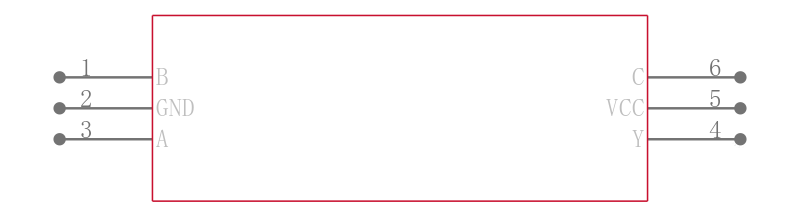
输出接口数 1
输出电流 20 mA
电路数 1
位数 1
传送延迟时间 8.30 ns
电压波节 3.30 V, 2.50 V, 1.80 V
逻辑门个数 1
输入数 3
工作温度Max 85 ℃
工作温度Min 40 ℃
电源电压 0.8V ~ 3.6V
电源电压Max 3.6 V
电源电压Min 0.8 V
安装方式 Surface Mount
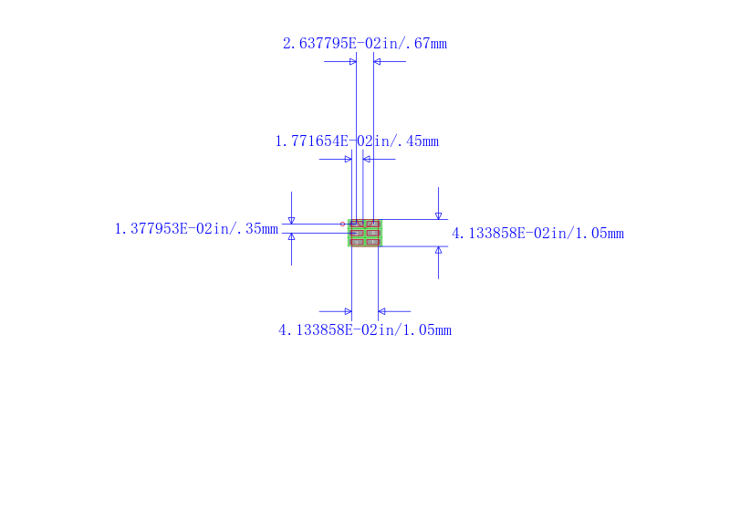
引脚数 6
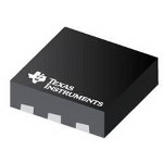
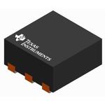
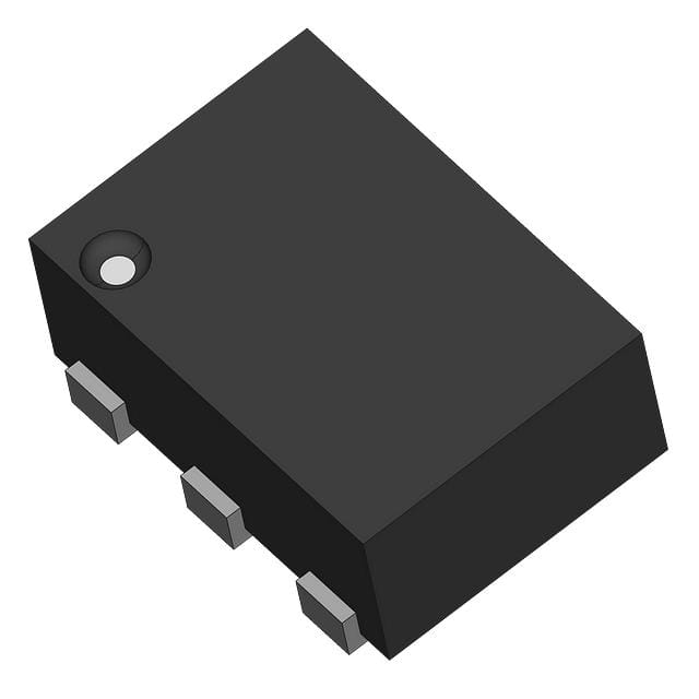
封装 X2SON-6
封装 X2SON-6
工作温度 -40℃ ~ 85℃
产品生命周期 Active
包装方式 Tape & Reel TR
RoHS标准 RoHS Compliant
含铅标准 Lead Free