


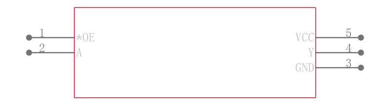
具有三态输出单总线缓冲器门 SINGLE BUS BUFFER GATE WITH 3-STATE OUTPUT
The is a single Bus Buffer Gate with 3-state outputs. The output is disabled when the output-enable OE input is high. The CMOS device has high output drive while maintaining low static power dissipation over a broad VCC operating range. The device contains one buffer gate device with output enable control and performs the Boolean function Y = A. This device is fully specified for partial-power-down applications using IOFF. The IOFF circuitry disables the outputs, preventing damaging current backflow through the device when it is powered down. To ensure the high-impedance state during power up or power down, OE should be tied to VCC through a pull-up resistor and the minimum value of the resistor is determined by the current-sinking capability of the driver.
- .
- Provides down translation to VCC
- .
- IOFF Supports live insertion, partial-power-down mode and back-drive protection
- .
- Latch-up performance exceeds 100mA per JESD 78, class II
- .
- Inputs accept voltages to 5.5V
- .
- 3.7ns at 3.3V Propagation delay tpd
- .
- 10µA ICC Low power consumption
- .
- ±24mA Output drive at 3.3V
- .
- Green product and no Sb/Br
电源电压DC -500 mV to 6.50 V
输出接口数 1
通道数 1
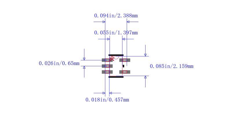
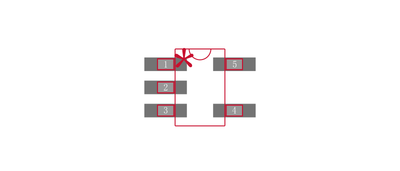
针脚数 5
位数 1
传送延迟时间 4.00 ns
逻辑门个数 1
输入数 1
工作温度Max 85 ℃
工作温度Min -40 ℃
电源电压 1.65V ~ 5.5V
电源电压Max 5.5 V
电源电压Min 1.65 V
安装方式 Surface Mount
引脚数 5
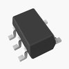
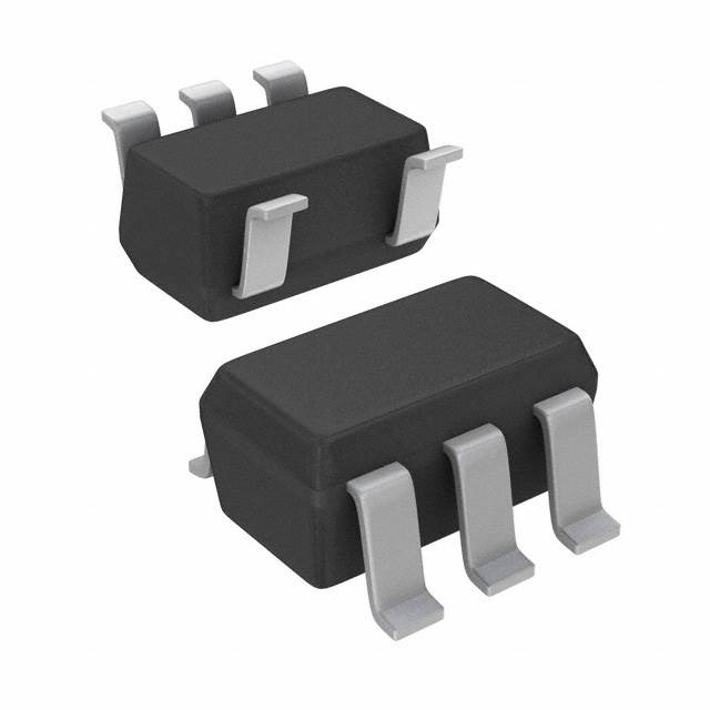
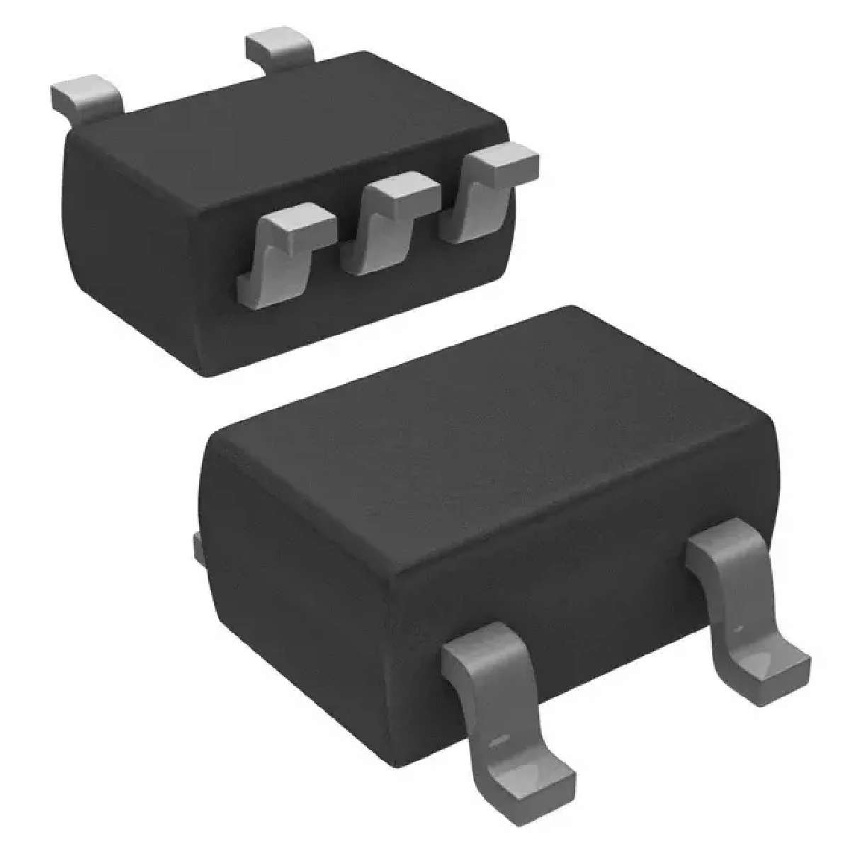
封装 SC-70-5
封装 SC-70-5
工作温度 -40℃ ~ 85℃
产品生命周期 Active
包装方式 Tape & Reel TR
制造应用 电机驱动与控制, 射频通信, 多媒体, 自动化与过程控制, 军用与航空, 通信与网络, 成像, 国防, 信号处理, 视频和目视, 计算机和计算机周边
RoHS标准 RoHS Compliant
含铅标准 Lead Free
REACH SVHC标准 No SVHC
军工级 Yes
REACH SVHC版本 2015/06/15
ECCN代码 EAR99
香港进出口证 NLR
| 型号/品牌 | 代替类型 | 替代型号对比 |
|---|---|---|
SN74LVC1G125DCKT TI 德州仪器 | 当前型号 | 当前型号 |
74LVC1G125DCKTE4 德州仪器 | 完全替代 | SN74LVC1G125DCKT和74LVC1G125DCKTE4的区别 |
74LVC1G125DCKTG4 德州仪器 | 完全替代 | SN74LVC1G125DCKT和74LVC1G125DCKTG4的区别 |
74LVC1G125DCKRE4 德州仪器 | 完全替代 | SN74LVC1G125DCKT和74LVC1G125DCKRE4的区别 |