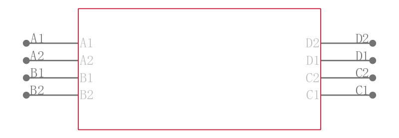


具有三态输出的双总线缓冲器门 DUAL BUS BUFFER GATE WITH 3-STATE OUTPUTS
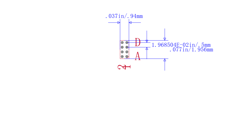
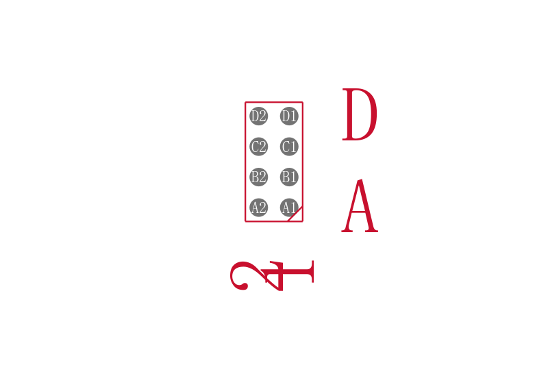
缓冲器,非反向 元件 1 位每元件 三态 Output 8-DSBGA,8-WCSP(1.9x0.9)
得捷:
IC BUF NON-INVERT 5.5V 8DSBGA
立创商城:
SN74LVC2G126YZPR
德州仪器TI:
2-ch, 1.65-V to 5.5-V buffers with 3-state outputs
艾睿:
This SN74LVC2G126YZPR buffer and line driver from Texas Instruments is used to amplify an analog or digital signal by driving the input to the transmission line. With a 3-state output, this is power management at its best. This line driver has a minimum operating temperature of -40 °C and a maximum of 125 °C. This component will be shipped in tape and reel packaging for effective mounting and safe delivery. It has 2 channels per chip. This non-inverting device has a typical operating supply voltage of 1.8|2.5|3.3|5 V. Its minimum operating supply voltage of 1.65 V, while its maximum is 5.5 V.
安富利:
Buffer/Line Driver 2-CH Non-Inverting 3-ST CMOS 8-Pin DSBGA T/R
Chip1Stop:
Buffer/Line Driver 2-CH Non-Inverting 3-ST CMOS 8-Pin DSBGA T/R
Verical:
Buffer/Line Driver 2-CH Non-Inverting 3-ST CMOS 8-Pin DSBGA T/R
Win Source:
IC BUS BUFF TRI-ST DL 8DSBGA
电源电压DC 1.65V ~ 5.50V
输出接口数 2
电路数 2
通道数 2
位数 2
传送延迟时间 3.20 ns
电压波节 5.00 V, 3.30 V, 2.50 V, 1.80 V
逻辑门个数 2
输出电流驱动 -1.00 mA
输入数 2
工作温度Max 125 ℃
工作温度Min -40 ℃
电源电压 1.65V ~ 5.5V
安装方式 Surface Mount
引脚数 8
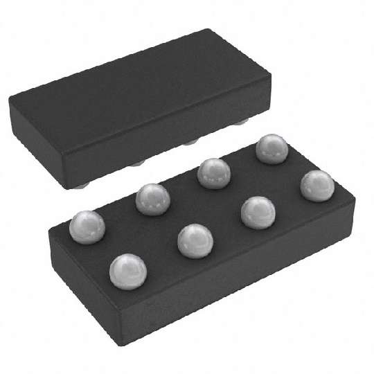
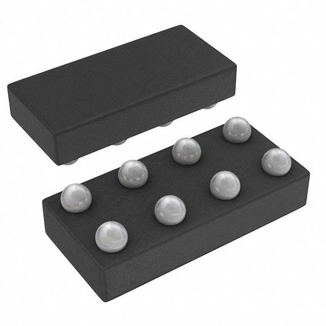
封装 DSBGA-8
封装 DSBGA-8
工作温度 -40℃ ~ 125℃ TA
产品生命周期 Active
包装方式 Tape & Reel TR
RoHS标准 RoHS Compliant
含铅标准 Lead Free
ECCN代码 EAR99