


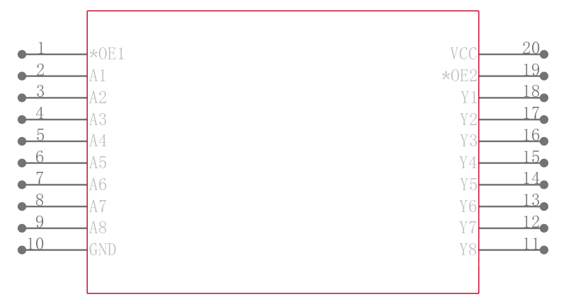
八路缓冲器/驱动器,具有三态输出 OCTAL BUFFER/DRIVER WITH 3-STATE OUTPUTS
DESCRIPON
The SN74LV541AT is designed for 4.5-V to 5.5-V VCC operation. The inputs are TTL-voltage compatible, which allows them to be interfaced with bipolar outputs and 3.3-V devices. The device also can be used to translate from 3.3 V to 5 V.
This device is ideal for driving bus lines or buffer memory address registers. It features inputs and outputs on opposite sides of the package to facilitate printed circuit board layout.
FEATURES
• Inputs Are TTL-Voltage Compatible
• 4.5-V to 5.5-V VCC Operation
• Typical tpd of 4 ns at 5 V
• Typical VOLP Output Ground Bounce
<0.8 V at VCC = 5 V, TA = 25°C
• Typical VOHV Output VOH Undershoot
>2.3 V at VCC = 5 V, TA = 25°C
• Supports Mixed-Mode Voltage Operation on All Ports
• Ioff Supports Partial-Power-Down Mode Operation
• Latch-Up Performance Exceeds 250 mA Per JESD 17
• ESD Protection Exceeds JESD 22
– 2000-V Human-Body Model A114-A
– 200-V Machine Model A115-A
– 1000-V Charged-Device Model C101
电源电压DC 4.50V ~ 5.50V
输出接口数 8
通道数 8
位数 8
传送延迟时间 7.90 ns
电压波节 5.00 V
输出电流驱动 -1.00 mA
输入数 8
工作温度Max 125 ℃
工作温度Min -40 ℃
电源电压 4.5V ~ 5.5V
安装方式 Surface Mount
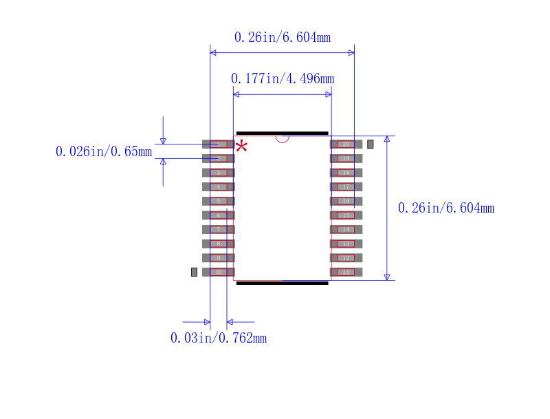
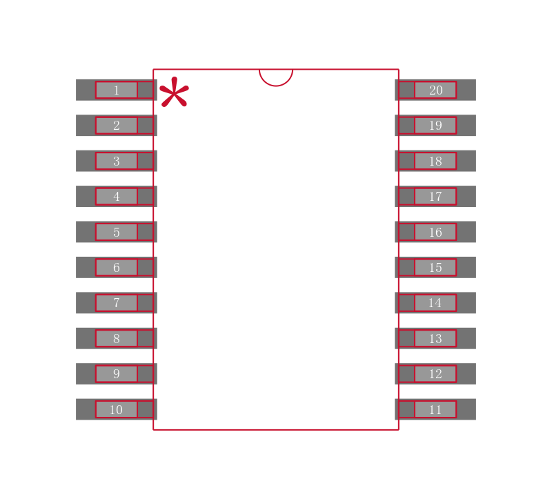
引脚数 20
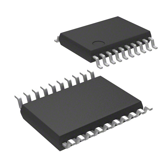
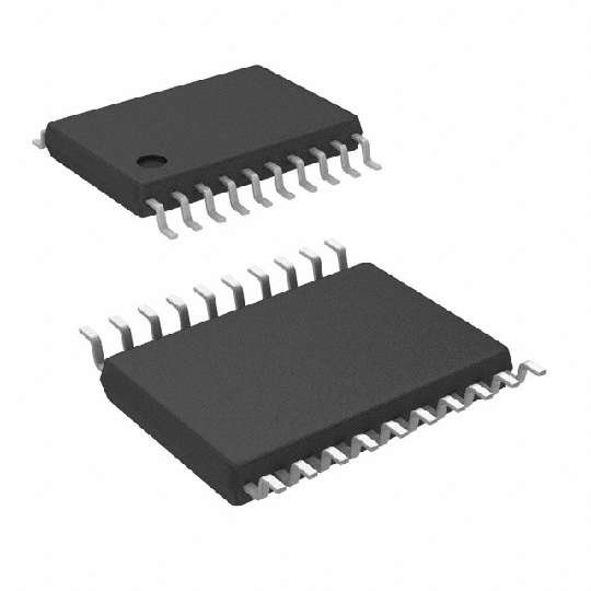
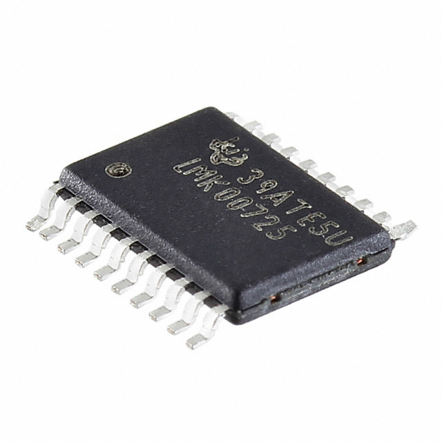
封装 TSSOP-20
长度 6.6 mm
宽度 4.5 mm
高度 1.05 mm
封装 TSSOP-20
工作温度 -40℃ ~ 125℃ TA
产品生命周期 Active
包装方式 Tape & Reel TR
RoHS标准 RoHS Compliant
含铅标准 Lead Free
REACH SVHC标准 No SVHC
| 型号/品牌 | 代替类型 | 替代型号对比 |
|---|---|---|
SN74LV541ATPWT TI 德州仪器 | 当前型号 | 当前型号 |
SN74LV541ATPW 德州仪器 | 完全替代 | SN74LV541ATPWT和SN74LV541ATPW的区别 |
SN74LV541ATPWG4 德州仪器 | 完全替代 | SN74LV541ATPWT和SN74LV541ATPWG4的区别 |
SN74LV541ATPWRE4 德州仪器 | 完全替代 | SN74LV541ATPWT和SN74LV541ATPWRE4的区别 |