


八路透明D类锁存器与三态输出 OCTAL TRANSPARENT D-TYPE LATCH WITH 3-STATE OUTPUTS
DESCRIPON/ORDERING INFORMATION
The SN74LVC373A octal transparent D-type latch is designed for 2.7-V to 3.6-V VCC operation. While the latch-enable LE input is high, the Q outputs follow the data D inputs. When LE is taken low, the Q outputs are latched at the logic levels set up at the D inputs.
A buffered output-enable OE input can be used to place the eight outputs in either a normal logic state high or low logic levels or the high-impedance state. In the high-impedance state, the outputs neither load nor drive the bus lines significantly. The high-impedance state and increased drive provide the capability to drive bus lines without interface or pullup components.
OE does not affect the internal operations of the latches. Old data can be retained or new data can be entered while the outputs are in the high-impedance state.
This device is fully specified for partial-power-down applications using Ioff. The Ioff circuitry disables the outputs, preventing damaging current backflow through the device when it is powered down.
FEATURES
• Qualified for Automotive Applications
• ESD Protection Exceeds 2000 V Per
MIL-STD-883, Method 3015; Exceeds 200 V
Using Machine Model C = 200 pF, R = 0
• Operates From 2 V to 3.6 V
• Inputs Accept Voltages to 5.5 V
• Max tpd of 7.5 ns at 3.3 V
• Typical VOLP Output Ground Bounce < 0.8 V at VCC = 3.3 V, TA = 25°C
• Typical VOHV Output VOH Undershoot > 2 V at VCC = 3.3 V, TA = 25°C
• Supports Mixed-Mode Signal Operation on All Ports 5-V Input/Output Voltage With 3.3-V VCC
• Ioff Supports Partial-Power-Down Mode Operation
电源电压DC 2.00V ~ 3.60V
输出接口数 8
电路数 1
位数 8
传送延迟时间 7.50 ns
电压波节 3.30 V, 2.70 V
输出电流驱动 -1.00 mA
工作温度Max 125 ℃
工作温度Min -40 ℃
电源电压 1.65V ~ 3.6V
电源电压Max 3.6 V
电源电压Min 2 V
安装方式 Surface Mount
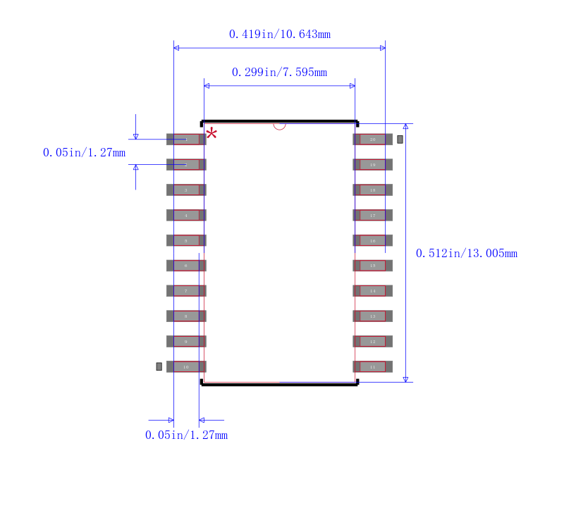
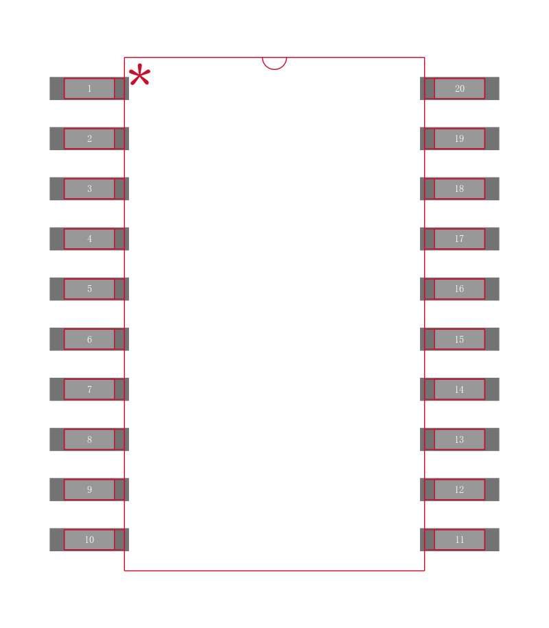
引脚数 20
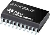
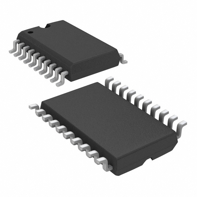
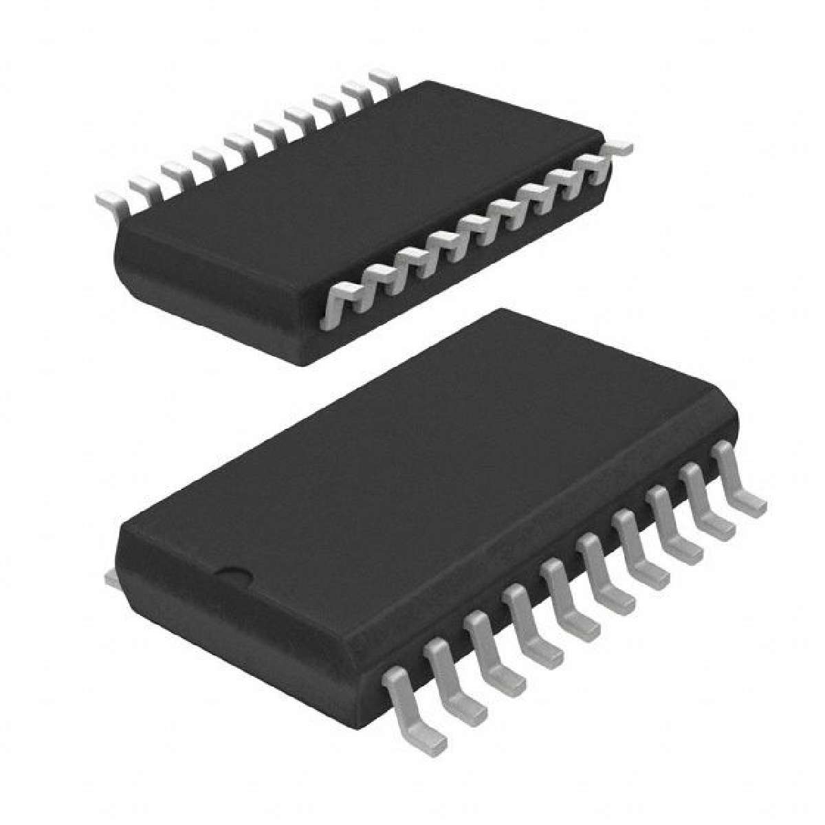
封装 SOIC-20
长度 12.8 mm
宽度 7.52 mm
高度 2.35 mm
封装 SOIC-20
工作温度 -40℃ ~ 125℃
产品生命周期 Obsolete
包装方式 Tape & Reel TR
RoHS标准 RoHS Compliant
含铅标准 Lead Free

| 型号/品牌 | 代替类型 | 替代型号对比 |
|---|---|---|
SN74LVC373AQDWRQ1 TI 德州仪器 | 当前型号 | 当前型号 |
SN74LVC373ADWR 德州仪器 | 类似代替 | SN74LVC373AQDWRQ1和SN74LVC373ADWR的区别 |
SN74LVC373ADWG4 德州仪器 | 类似代替 | SN74LVC373AQDWRQ1和SN74LVC373ADWG4的区别 |
CLVC373AQDWRG4Q1 德州仪器 | 类似代替 | SN74LVC373AQDWRQ1和CLVC373AQDWRG4Q1的区别 |