


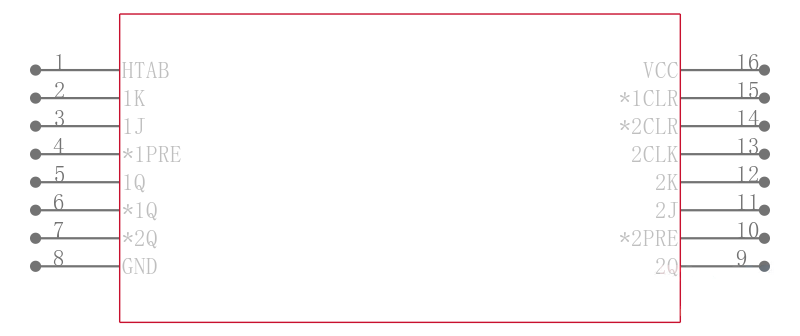
触发器 Dual Neg-Edge-Trig J-K Flip-Flop
description/ordering information
The ’HC112 devices contain two independent J-K negative-edge-triggered flip-flops. A low level at the preset PRE or clear CLR inputs sets or resets the outputs, regardless of the levels of the other inputs. When PRE and CLR are inactive high, data at the J and K inputs meeting the setup time requirements are transferred to the outputs on the negative-going edge of the clock CLK pulse. Clock triggering occurs at a voltage
• Wide Operating Voltage Range of 2 V to 6 V
• Outputs Can Drive Up To 10 LSTTL Loads
• Low Power Consumption, 40-µA Max ICC
• Typical tpd = 13 ns
• ±4-mA Output Drive at 5 V
• Low Input Current of 1 µA Max
频率 60.0 MHz
电源电压DC 2.00V ~ 6.00V
输出接口数 1
输出电流 5.20 mA
电路数 2
时钟频率 60 MHz
位数 2
传送延迟时间 26.0 ns
电压波节 6.00 V, 5.00 V, 2.00 V
输入电容 3 pF
输出电流驱动 -1.00 mA
输入数 2
工作温度Max 85 ℃
工作温度Min -40 ℃
电源电压 2V ~ 6V
安装方式 Surface Mount
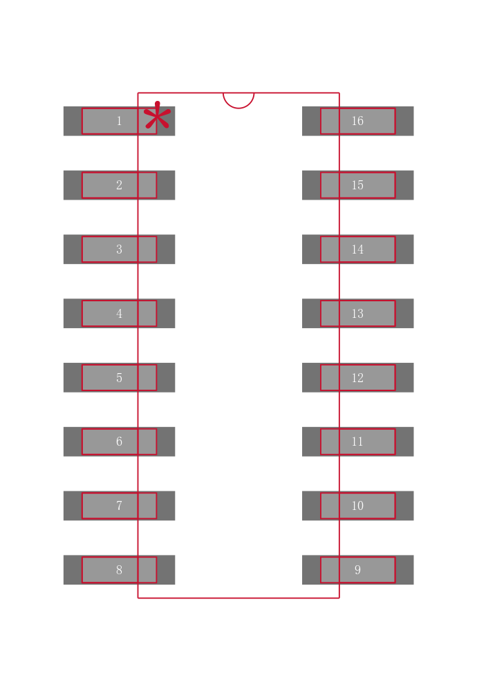
引脚数 16
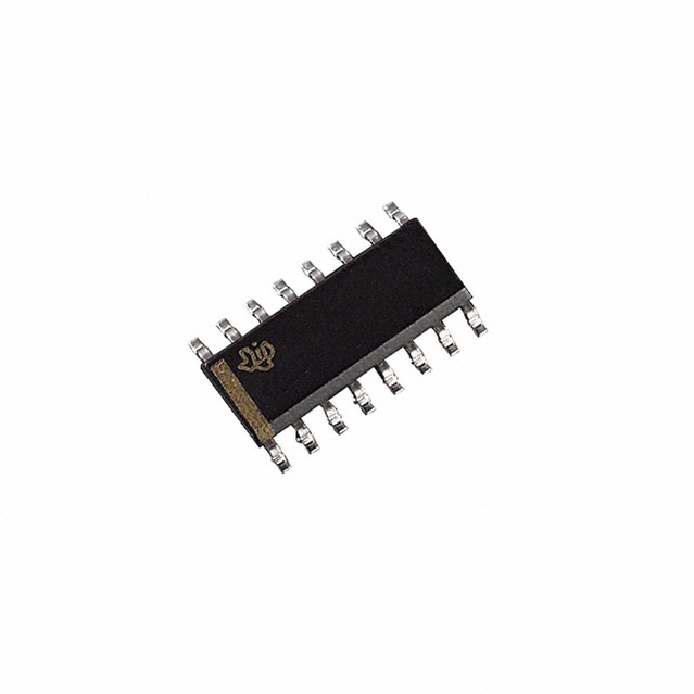
封装 SOIC-16
长度 9.9 mm
宽度 3.91 mm
高度 1.5 mm
封装 SOIC-16
工作温度 -40℃ ~ 85℃ TA
产品生命周期 Active
包装方式 Tube
RoHS标准 RoHS Compliant
含铅标准 Lead Free

| 型号/品牌 | 代替类型 | 替代型号对比 |
|---|---|---|
SN74HC112DE4 TI 德州仪器 | 当前型号 | 当前型号 |
SN74HC112D 德州仪器 | 类似代替 | SN74HC112DE4和SN74HC112D的区别 |
SN74HC112DR 德州仪器 | 类似代替 | SN74HC112DE4和SN74HC112DR的区别 |