
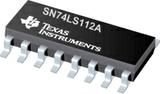


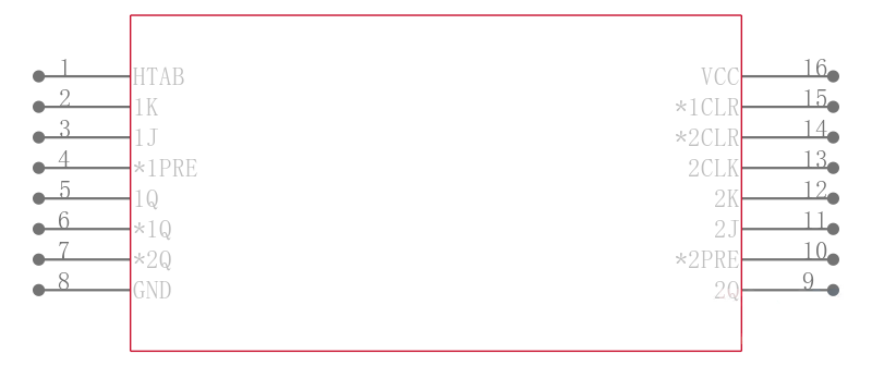
双JK负边沿触发触发器WIITH预置和清除 DUAL J-K NEGATIVE-EDGE-TRIGGERED FLIP-FLOPS WIITH PRESET AND CLEAR
These devices contain two independent J-K negative-edge-triggered flip-flops. A low level at the preset and clear inputs sets or resets the outputs regardless of the levels of the other inputs. When preset and clear are inactive high, data at the J and K inputs meeting the setup time requirements are transferred to the outputs on the negative-going edge of the clock pulse. Clock triggering occurs at a voltage level and is not directly related to the rise time of the clock pulse. Following the hold time interval, data at the J and K inputs may be changed without affecting the levels at the outputs. These versatile flip-flops can perform as toggle flip-flops by tying J and K high.
The SN54LS112A and SN54S112 are characterized for operation over the full military temperature range of -55°C to 125°C. The SN74LS112A and SN74S112A are characterized for operation from 0°C to 70°C.
View datasheet View product folder
频率 45 MHz
电源电压DC 4.75V ~ 5.25V
输出接口数 1
输出电流 8.00 mA
电路数 2
时钟频率 45 MHz
位数 2
传送延迟时间 20.0 ns
极性 Non-Inverting, Inverting
电压波节 5.00 V
输出电流驱动 -50.0 µA
输入数 2
工作温度Max 70 ℃
工作温度Min 0 ℃
电源电压 4.75V ~ 5.25V
安装方式 Surface Mount
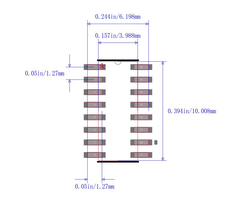
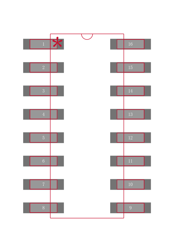
引脚数 16
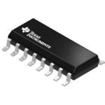
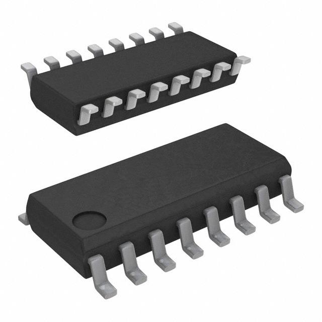
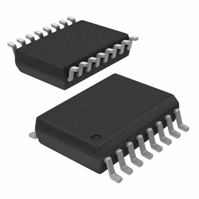
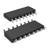
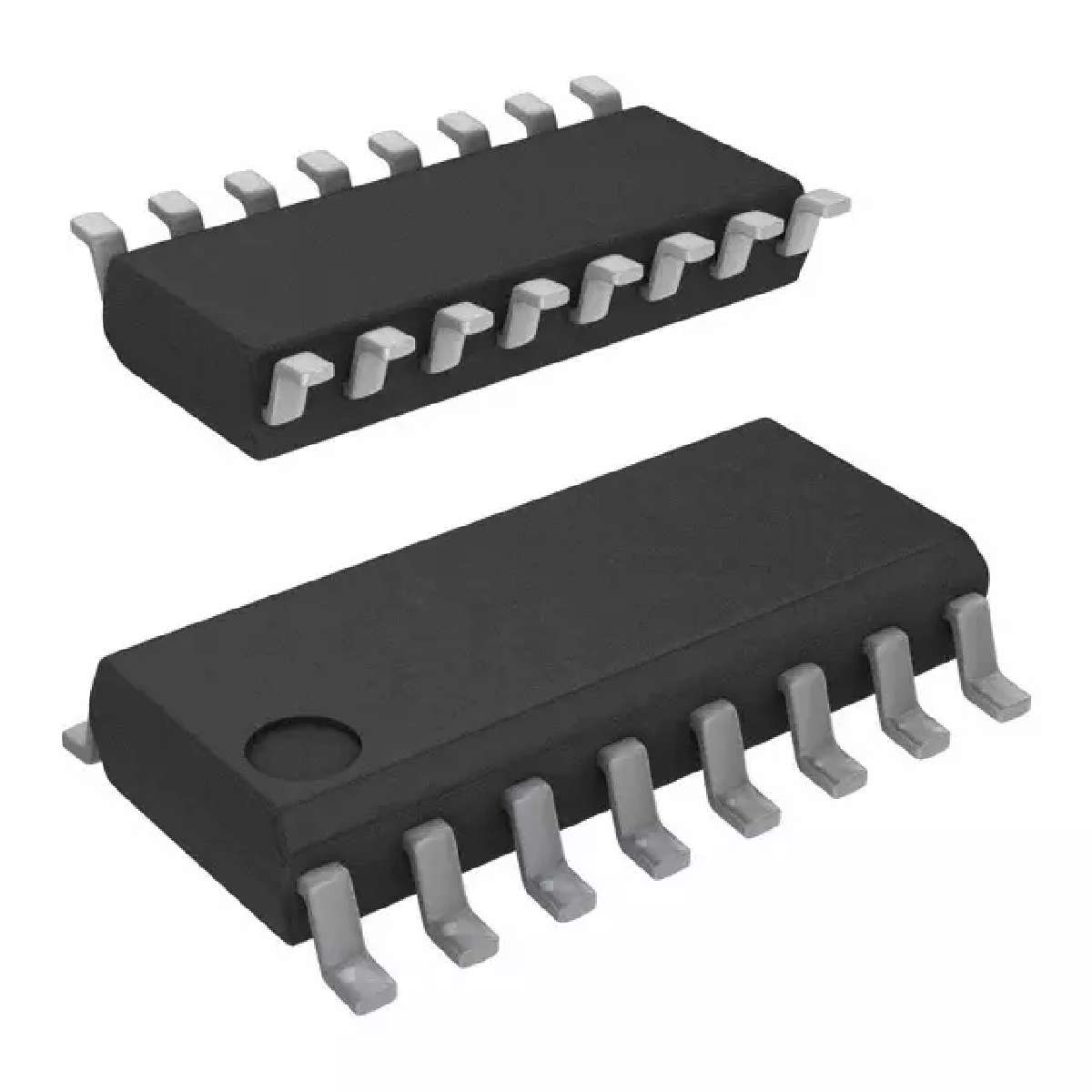
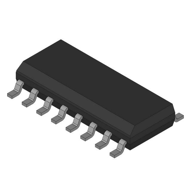
封装 SOIC-16
封装 SOIC-16
工作温度 0℃ ~ 70℃ TA
产品生命周期 Active
包装方式 Tape & Reel TR
RoHS标准 RoHS Compliant
含铅标准 Lead Free
| 型号/品牌 | 代替类型 | 替代型号对比 |
|---|---|---|
SN74LS112ADR TI 德州仪器 | 当前型号 | 当前型号 |
SN74LS174D 德州仪器 | 类似代替 | SN74LS112ADR和SN74LS174D的区别 |
SN74LS174DR 德州仪器 | 类似代替 | SN74LS112ADR和SN74LS174DR的区别 |
SN74LS112AD 德州仪器 | 类似代替 | SN74LS112ADR和SN74LS112AD的区别 |