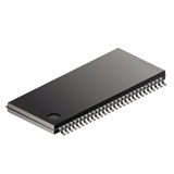
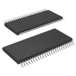
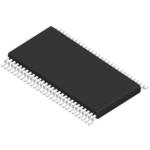
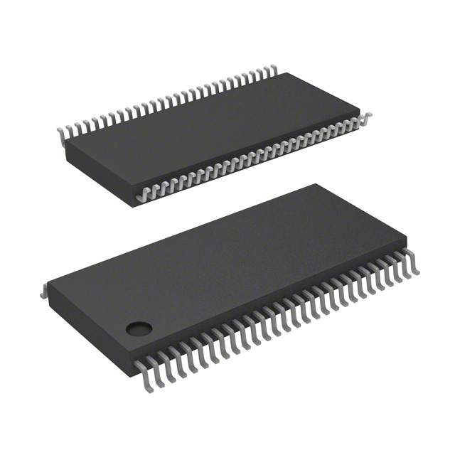


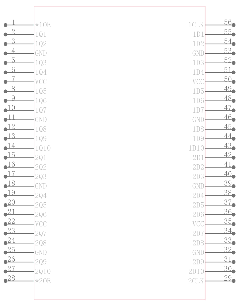
具有三态输出的 2.5V/3.3V 20 位总线接口触发器 56-TSSOP -40 to 85
The "ALVTH16821 devices are 20-bit bus-interface flip-flops with 3-state outputs designed for 2.5-V or 3.3-V VCC operation, but with the capability to provide a TTL interface to a 5-V system environment.
The devices can be used as two 10-bit flip-flops or one 20-bit flip-flop. The 20-bit flip-flops are edge-triggered D-type flip-flops. On the positive transition of the clock CLK, the flip-flops store the logic levels set up at the D inputs.
A buffered output-enable OE\\\\ input can be used to place the ten outputs in either a normal logic state high or low level or a high-impedance state. In the high-impedance state, the outputs neither load nor drive the bus lines significantly. The high-impedance state and increased drive provide the capability to drive bus lines without need for interface or pullup components.
OE\ does not affect the internal operation of the flip-flops. Old data can be retained or new data can be entered while the outputs are in the high-impedance state.
When VCC is between 0 and 1.2 V, the device is in the high-impedance state during power up or power down. However, to ensure the high-impedance state above 1.2 V, OE\ should be tied to VCC through a pullup resistor; the minimum value of the resistor is determined by the current-sinking capability of the driver.
Active bus-hold circuitry is provided to hold unused or floating data inputs at a valid logic level.
The SN54ALVTH16821 is characterized for operation over the full military temperature range of -55°C to 125°C. The SN74ALVTH16821 is characterized for operation from -40°C to 85°C.
频率 150 MHz
电源电压DC 3.30 V, 3.60 V max
输出接口数 10
输出电流 64.0 mA
时钟频率 150 MHz
位数 20
极性 Non-Inverting
电压波节 3.30 V, 2.50 V
输入电容 3.5 pF
输入数 10
工作温度Max 85 ℃
工作温度Min -40 ℃
安装方式 Surface Mount
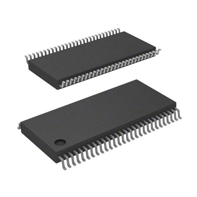
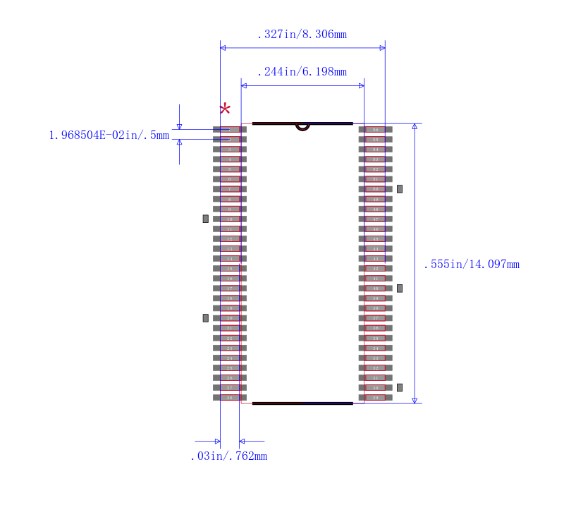
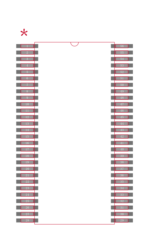
引脚数 56
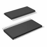
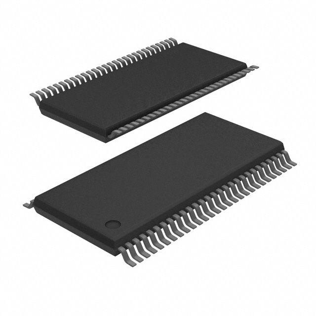
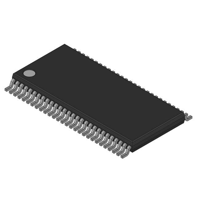
封装 TSSOP-56
封装 TSSOP-56
工作温度 -40℃ ~ 85℃ TA
产品生命周期 Active
包装方式 Tape & Reel TR
RoHS标准 RoHS Compliant
含铅标准 Lead Free
| 型号/品牌 | 代替类型 | 替代型号对比 |
|---|---|---|
SN74ALVTH16821GR TI 德州仪器 | 当前型号 | 当前型号 |
SN74ALVTH16821DLR 德州仪器 | 完全替代 | SN74ALVTH16821GR和SN74ALVTH16821DLR的区别 |
SN74ALVTH16821VR 德州仪器 | 完全替代 | SN74ALVTH16821GR和SN74ALVTH16821VR的区别 |
SN74ALVTH16821DL 德州仪器 | 类似代替 | SN74ALVTH16821GR和SN74ALVTH16821DL的区别 |