


具有三态输出的12位线/ MEMORY DRIVERS 12-BIT LINE/MEMORY DRIVERS WITH 3-STATE OUTPUTS
description
These 12-bit buffers and line drivers are designed specifically to improve both the performance and density of 3-state memory address drivers, clock drivers, and bus-oriented receivers and transmitters.
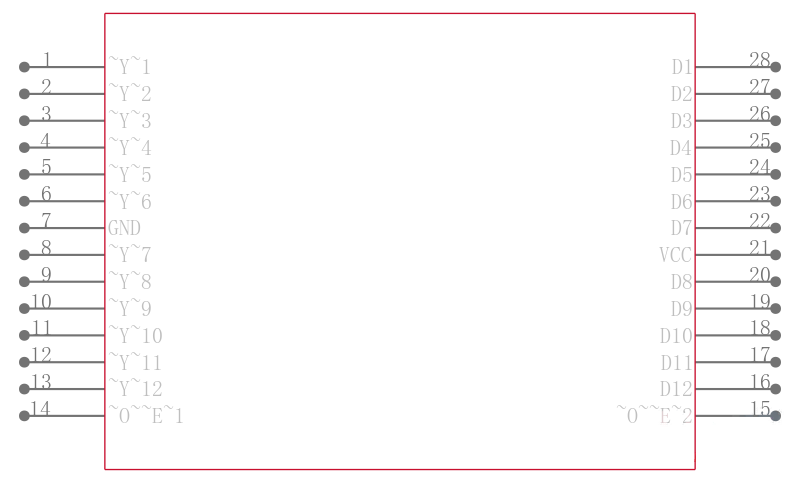
The 3-state control gate is a 2-input AND gate with active-low inputs so that if either output-enable OE1 or OE2 input is high, all 12 outputs are in the high-impedance state. These devices provide inverted data.
The outputs, which are designed to source or sink up to 12 mA, include equivalent 25-Ω series resistors to reduce overshoot and undershoot.
To ensure the high-impedance state during power up or power down, OE should be tied to VCC through a pullup resistor; the minimum value of the resistor is determined by the current-sinking capability of the driver.
The SN54ABT5403 is characterized for operation over the full military temperature range of –55°C to 125°C.
The SN74ABT5403 is characterized for operation from –40°C to 85°C.
• Output Ports Have Equivalent 25-Ω Series Resistors, So No External Resistors Are Required
• State-of-the-Art EPIC-ΙΙB BiCMOS Design Significantly Reduces Power Dissipation
• Latch-Up Performance Exceeds 500 mA Per JEDEC Standard JESD-17
• Typical VOLP Output Ground Bounce < 1 V at VCC = 5 V, TA = 25°C
• Typical VOLV Output Undershoot < 0.5 V at VCC = 5 V, TA = 25°C
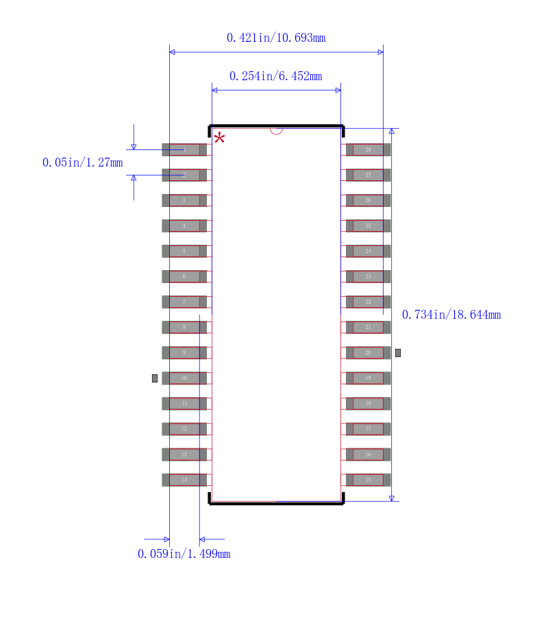
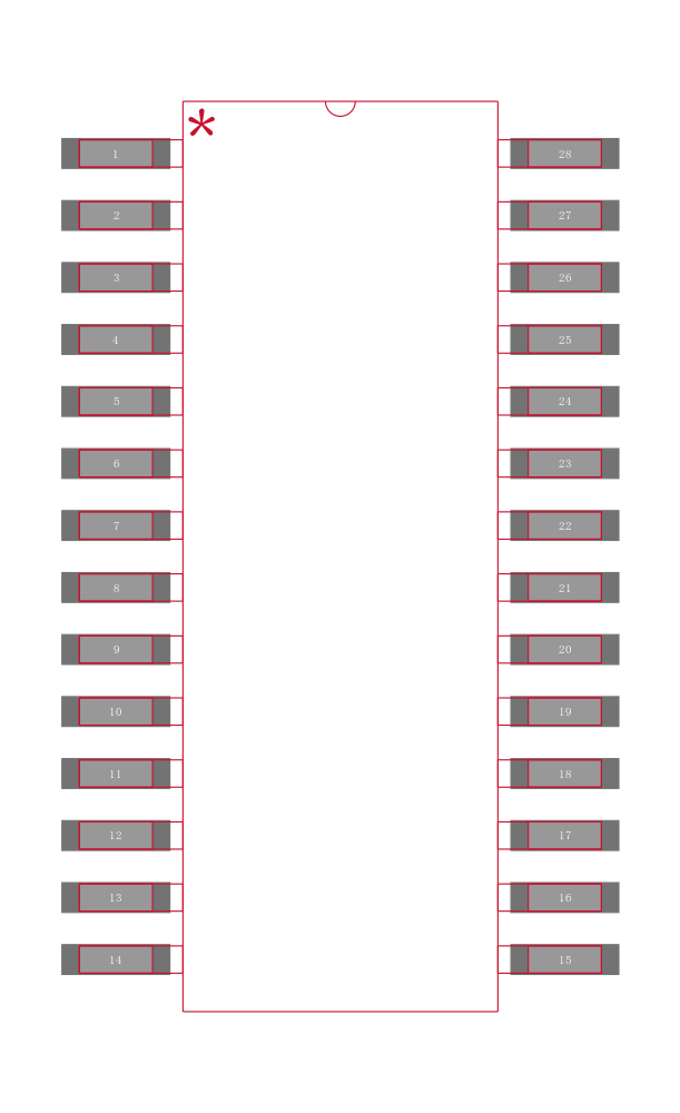
• Package Options Include Plastic Small-Outline DW Package, Ceramic Chip Carriers FK, and DIPs JT
| 型号/品牌 | 代替类型 | 替代型号对比 |
|---|---|---|
SN74ABT5403DW TI 德州仪器 | 当前型号 | 当前型号 |
SN74ABT5403DWR 德州仪器 | 完全替代 | SN74ABT5403DW和SN74ABT5403DWR的区别 |
SN74ABT5403DWE4 德州仪器 | 完全替代 | SN74ABT5403DW和SN74ABT5403DWE4的区别 |
SN74ABT5403DWG4 德州仪器 | 完全替代 | SN74ABT5403DW和SN74ABT5403DWG4的区别 |