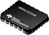

八路边沿触发D型触发器具有三态输出 OCTAL EDGE-TRIGGERED D-TYPE FLIP-FLOPS WITH 3-STATE OUTPUTS
description/ordering information
The SN54LVC574A octal edge-triggered D-type flip-flop is designed for 2.7-V to 3.6-V VCC operation, and the SN74LVC574A octal edge-triggered D-type flip-flop is designed for 1.65-V to 3.6-V VCC operation. These devices feature 3-state outputs designed specifically for driving highly capacitive or relatively low-impedance loads. They are particularly suitable for implementing buffer registers, I/O ports, bidirectional bus drivers, and working registers.
Operate From 1.65 V to 3.6 V
Inputs Accept Voltages to 5.5 V
Specified From −40°C to 85°C,−40°C to 125°C, and −55°C to 125°C
Max tpd of 7 ns at 3.3 V
Typical VOLP Output Ground Bounce <0.8 V at VCC = 3.3 V, TA = 25°C
Typical VOHV Output VOH Undershoot >2 V at VCC = 3.3 V, TA = 25°C
Support Mixed-Mode Signal Operation on All Ports 5-V Input/Output Voltage With 3.3-V VCC
Ioff Supports Partial-Power-Down Mode Operation
Latch-Up Performance Exceeds 250 mA Per JESD 17
ESD Protection Exceeds JESD 22
− 2000-V Human-Body Model A114-A
− 200-V Machine Model A115-A
− 1000-V Charged-Device Model C101
频率 150 MHz
电源电压DC 2.00V ~ 3.60V
输出接口数 8
位数 8
传送延迟时间 7.00 ns
电压波节 3.30 V, 2.70 V, 2.50 V, 1.80 V
输出电流驱动 -1.00 mA
输入数 8
工作温度Max 125 ℃
工作温度Min -55 ℃
安装方式 Surface Mount
引脚数 20
封装 CFPAK
封装 CFPAK
工作温度 -55℃ ~ 125℃
产品生命周期 Active
包装方式 Tube
RoHS标准 Non-Compliant
含铅标准 Contains Lead
ECCN代码 EAR99
| 型号/品牌 | 代替类型 | 替代型号对比 |
|---|---|---|
SNJ54LVC574AW TI 德州仪器 | 当前型号 | 当前型号 |
5962-9757601QSA 德州仪器 | 完全替代 | SNJ54LVC574AW和5962-9757601QSA的区别 |