
八路边沿触发D型触发器具有三态输出 OCTAL EDGE-TRIGGERED D-TYPE FLIP-FLOPS WITH 3-STATE OUTPUTS
description/ordering information
The ’LV574A devices are octal edge-triggered D-type flip-flops designed for 2-V to 5.5-V VCC operation.
These devices feature 3-state outputs designed specifically for driving highly capacitive or relatively low-impedance loads. The devices are particularly suitable for implementing buffer registers, I/O ports, bidirectional bus drivers, and working registers.
On the positive transition of the clock CLK input, the Q outputs are set to the logic levels set up at the data D inputs.
A buffered output-enable OE input can be used to place the eight outputs in either a normal logic state high or low logic levels or high-impedance state. In the high-impedance state, the outputs neither load nor drive the bus lines significantly. The high-impedance state and increased drive provide the capability to drive bus lines without need for interface or pullup components.
2-V to 5.5-V VCCOperation
Max tpdof 10 ns at 5 V
Typical VOLPOutput Ground Bounce
<0.8 V at VCC= 3.3 V, TA= 25°C
Typical VOHVOutput VOHUndershoot
>2.3 V at VCC= 3.3 V, TA= 25°C
Support Mixed-Mode Voltage Operation on All Ports
Ioff Supports Partial-Power-Down Mode Operation
Latch-Up Performance Exceeds 250 mA Per JESD 17
ESD Protection Exceeds JESD 22
− 2000-V Human-Body Model A114-A
− 200-V Machine Model A115-A
− 1000-V Charged-Device Model C101
电源电压DC 5.00 V, 5.50 V max
电路数 8
时钟频率 205 MHz
位数 8
极性 Non-Inverting
电压波节 5.00 V, 3.30 V, 2.50 V
输入电容 1.8 pF
工作温度Max 85 ℃
工作温度Min -40 ℃
电源电压 2V ~ 5.5V
安装方式 Surface Mount
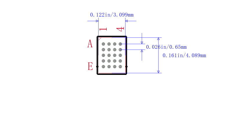
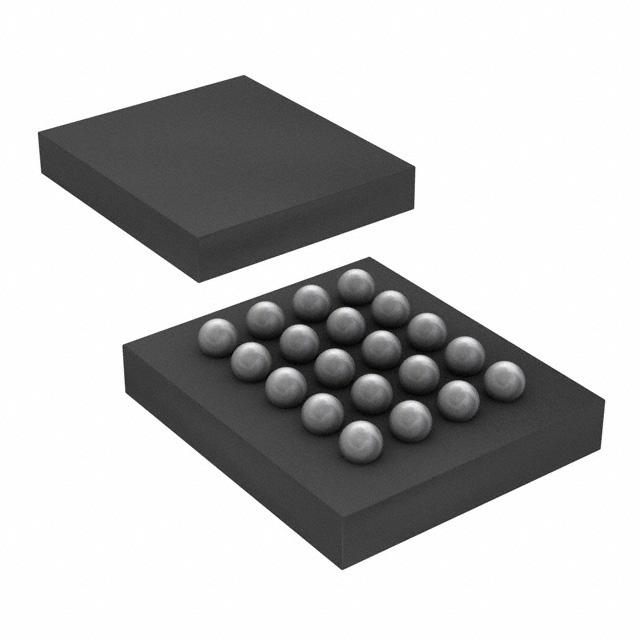
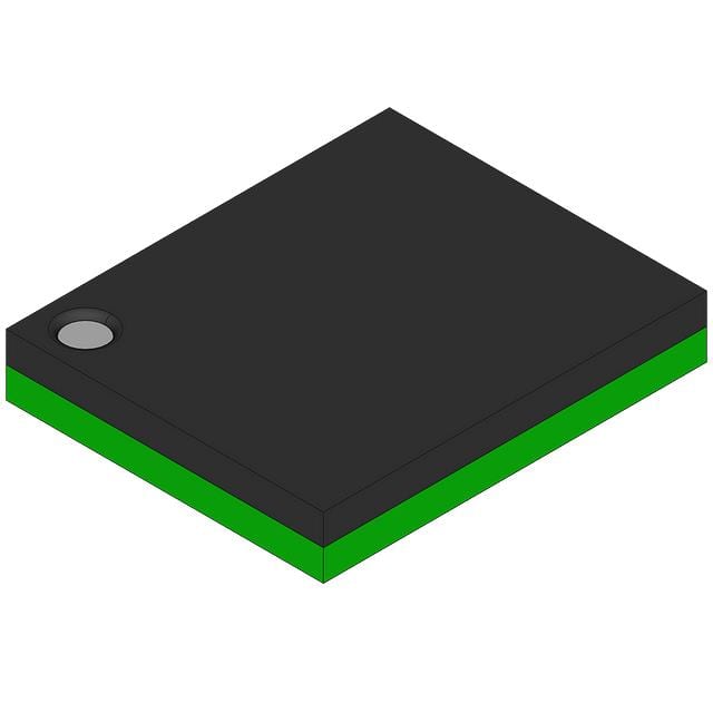
引脚数 20
封装 VFBGA-20
长度 4 mm
宽度 3 mm
高度 0.75 mm
封装 VFBGA-20
工作温度 -40℃ ~ 85℃ TA
产品生命周期 Not Recommended for New Designs
包装方式 Tape & Reel TR
RoHS标准 Non-Compliant
含铅标准 Contains Lead