

2.5 V / 3.3 V振荡器增益级/缓冲区 2.5-V/3.3-V OSCILLATOR GAIN STAGE/BUFFERS
DESCRIPON
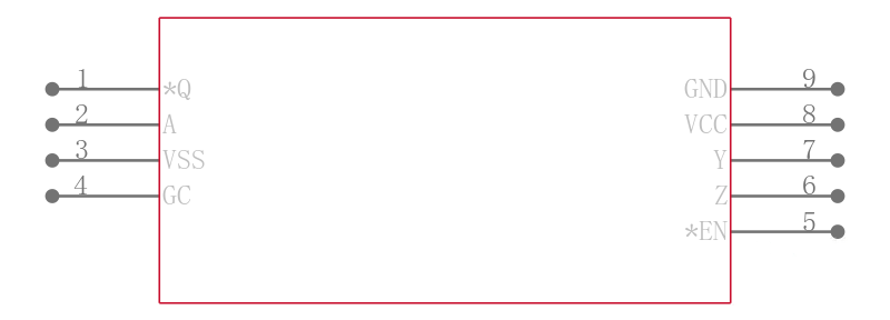
These four devices are high-frequency oscillator gain stages supporting both LVPECL or LVDS on the high gain outputs in 3.3-V or 2.5-V systems. Additionally, provides the option of both single-ended input PECL levels on the SN65LVx16 and fully differential inputs on the SN65LVx17.
FEATURES
• Low-Voltage PECL Input and Low-Voltage PECL or LVDS Outputs
• Clock Rates to 2 GHz
– 140-ps Output Transition Times
– 0.11 ps Typical Intrinsic Phase Jitter
– Less than 630 ps Propagation Delay Times
• 2.5-V or 3.3-V Supply Operation
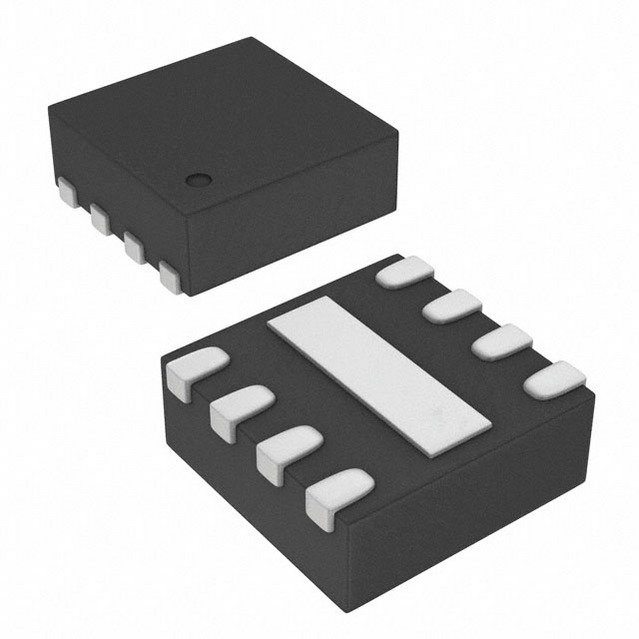
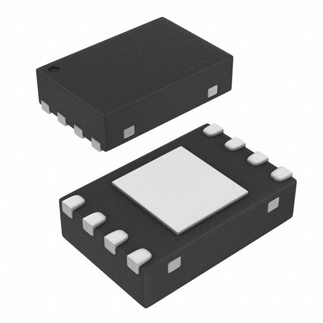
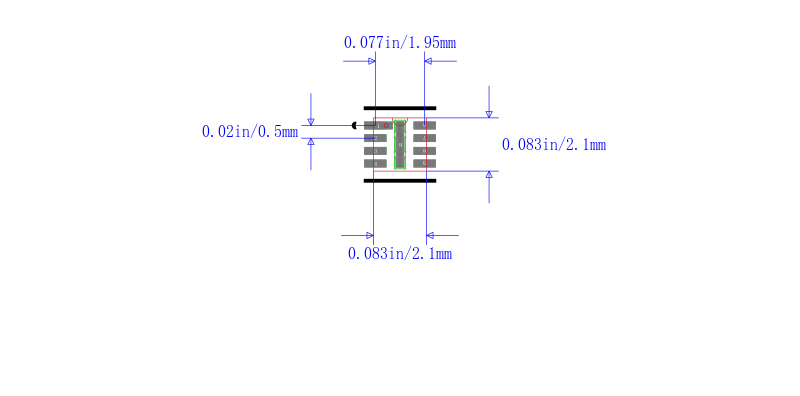
• 2-mm × 2-mm Small-Outline No-Lead Package
APPLICATIONS
• PECL-to-LVDS Translation
• Clock Signal Amplification

| 型号/品牌 | 代替类型 | 替代型号对比 |
|---|---|---|
SN65LVDS16DRFR TI 德州仪器 | 当前型号 | 当前型号 |
SN65LVDS16DRFT 德州仪器 | 类似代替 | SN65LVDS16DRFR和SN65LVDS16DRFT的区别 |