


INFINEON SPD15P10PGBTMA1 晶体管, 射频FET, -100 V, -15 A, 128 W, TO-252
SIPMOS® P 通道 MOSFET
**Infineon** SIPMOS® 小信号 P 通道 MOSFET 具有多种功能,可能包括增强模式、连续漏极电流(约低至 80A)及宽工作温度范围。 SIPMOS 功率可用于多种应用,包括电信、eMobility、笔记本、直流/直流设备以及汽车工业。
· 符合 AEC Q101 标准(请参阅数据表)
· 无铅引线电镀,符合 RoHS 标准
得捷:
MOSFET P-CH 100V 15A TO252-3
欧时:
Infineon SIPMOS 系列 Si P沟道 MOSFET SPD15P10PGBTMA1, 15 A, Vds=100 V, 3引脚 DPAK TO-252封装
立创商城:
P沟道 100V 15A
贸泽:
MOSFET P-Ch -100V 15A DPAK-2
艾睿:
Thanks to Infineon Technologies, both your amplification and switching needs can be taken care of with one component: the SPD15P10PGBTMA1 power MOSFET. Its maximum power dissipation is 128000 mW. This component will be shipped in tape and reel packaging to allow for effective mounting and safe delivery. This P channel MOSFET transistor operates in enhancement mode. This MOSFET transistor has a minimum operating temperature of -55 °C and a maximum of 175 °C. This device is made with sipmos technology.
TME:
Transistor: P-MOSFET; unipolar; -100V; -15A; 128W; PG-TO252-3
Verical:
Trans MOSFET P-CH 100V 15A Automotive 3-Pin2+Tab DPAK T/R
Newark:
# INFINEON SPD15P10PGBTMA1 RF FET Transistor, -100 V, -15 A, 128 W, TO-252
Win Source:
MOSFET P-CH 100V 15A TO252-3
额定功率 128 W
针脚数 3
极性 P-Channel
耗散功率 128 W
漏源极电压Vds 100 V
连续漏极电流Ids 15A
上升时间 23 ns
输入电容Ciss 1280pF @25VVds
下降时间 16 ns
工作温度Max 175 ℃
工作温度Min -55 ℃
耗散功率Max 128W Tc
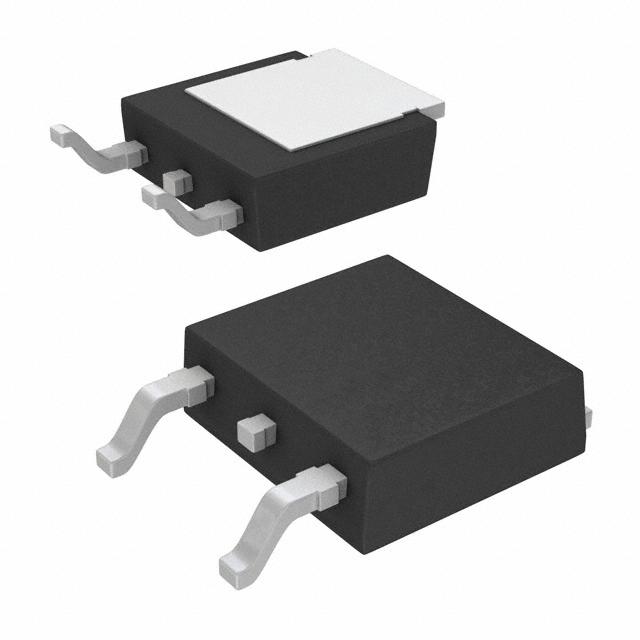
安装方式 Surface Mount
引脚数 3
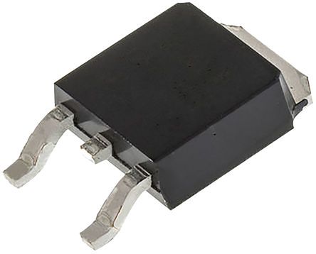
封装 TO-252-3
长度 6.73 mm
宽度 6.22 mm
高度 2.41 mm
封装 TO-252-3
工作温度 -55℃ ~ 175℃ TJ
产品生命周期 Active
包装方式 Tape & Reel TR
制造应用 Power Management, Onboard charger, 电机驱动与控制, 车用, Automotive, Consumer Electronics, 计算机和计算机周边, Computers & Computer Peripherals, 电源管理, Motor Drive & Control, 消费电子产品
RoHS标准 RoHS Compliant
含铅标准 Lead Free
REACH SVHC标准 No SVHC
REACH SVHC版本 2015/12/17