


翻两番总线缓冲器闸3态输出 QUADRUPLE BUS BUFFER GATES WITH 3 STATE OUTPUTS
description/ordering information
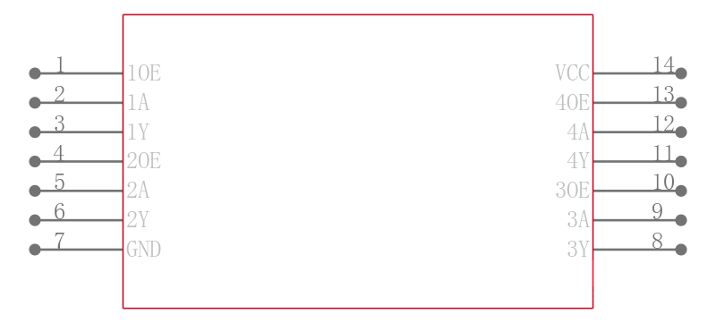
These quadruple bus buffer gates are designed for 2-V to 5.5-V VCC operation. The ’LV126A devices feature independent line drivers with 3-state outputs. Each output is disabled when the associated output-enable OE input is low. To ensure the high-impedance state during power up or power down, OE should be tied to GND through a pulldown resistor; the minimum value of the resistor is determined by the current-sourcing capability of the driver.
2-V to 5.5-V VCC Operation
Max tpd of 6.5 ns at 5 V
Typical VOLPOutput Ground Bounce
<0.8 V at VCC = 3.3 V, TA= 25°C
Typical VOHVOutput VOHUndershoot
>2.3 V at VCC = 3.3 V, TA= 25°C
Support Mixed-Mode Voltage Operation on All Ports
Latch-Up Performance Exceeds 250 mA Per JESD 17
ESD Protection Exceeds JESD 22
− 2000-V Human-Body Model A114-A
− 200-V Machine Model A115-A
− 1000-V Charged-Device Model C101
| 型号/品牌 | 代替类型 | 替代型号对比 |
|---|---|---|
SN74LV126APWG4 TI 德州仪器 | 当前型号 | 当前型号 |
SN74LV126APW 德州仪器 | 类似代替 | SN74LV126APWG4和SN74LV126APW的区别 |
SN74LV367APWR 德州仪器 | 类似代替 | SN74LV126APWG4和SN74LV367APWR的区别 |
SN74LV367APWT 德州仪器 | 类似代替 | SN74LV126APWG4和SN74LV367APWT的区别 |