
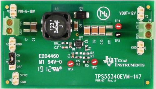

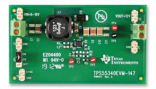
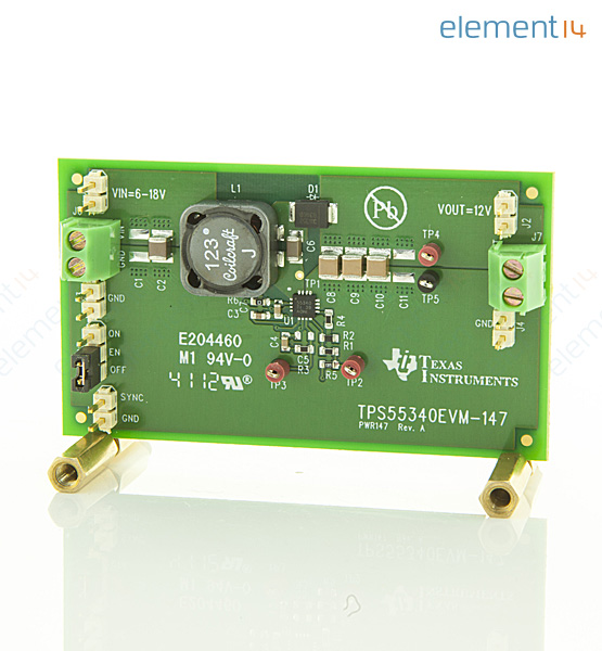
TPS55340EVM - 147 , 6V至18V输入, 12V输出SEPIC评估模块 TPS55340EVM-147, 6V to 18V Input, 12V Output SEPIC Evaluation Module
The is an evaluation module helps the designers to evaluate the performance of the TPS55340 DC/DC boost converter in a SEPIC topology. This evaluation module demonstrates the performance of the TPS55340 in an example application and can accommodate evaluation of other SEPIC applications supported by the TPS55340. This design shows a small printed circuit board area that can be achieved when designing with the TPS55340 regulator. However, appropriate sizing of the inductor and diode for the desired application can further reduce the board area. The switching frequency is externally set at a nominal 500kHz. The 40V, 5A, low side MOSFET is incorporated inside the TPS55340 package along with the gate drive circuitry. The low drain to source on resistance of the MOSFET allows the TPS55340 to achieve high efficiencies. The compensation components are external to the integrated circuit. The absolute maximum input voltage for the evaluation module is 26V.
- .
- Integrated 40V, 5A low side FET
- .
- High efficiency with 60mR internal FET
- .
- Cycle by cycle current limit with frequency fold back
- .
- Cycle skipping for output regulation at light loads
- .
- Adjustable soft start and switching frequency
- .
- Synchronization capability to external clock
- .
- Frequency adjustable from 100KHz to 1.2MHz