

系列低功耗轨至轨输入/输出运算放大器,带有关断的 FAMILY OF LOW-POWER RAIL-TO-RAIL INPUT/OUTPUT OPERATIONAL AMPLIFIERS WITH SHUTDOWN
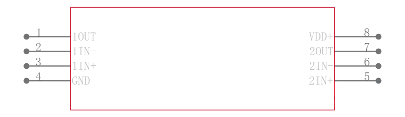
The TLV246x is a family of low-power rail-to-rail input/output operational amplifiers specifically designed for portable applications. The input common-mode voltage range extends beyond the supply rails for maximum dynamic range in low-voltage systems. The amplifier output has rail-to-rail performance with high-output-drive capability, solving one of the limitations of older rail-to-rail input/output operational amplifiers. This rail-to-rail dynamic range and high output drive make the TLV246x ideal for buffering analog-to-digital converters.
The operational amplifier has 6.4 MHz of bandwidth and 1.6 V/µs of slew rate with only 500 µA of supply current, providing good ac performance with low power consumption. Three members of the family offer a shutdown terminal, which places the amplifier in an ultralow supply current mode IDD = 0.3 µA/ch. While in shutdown, the operational-amplifier output is placed in a high-impedance state. DC applications are also well served with an input noise voltage of 11 nV/Hz and input offset voltage of 100 µV.
This family is available in the low-profile SOT23, MSOP, and TSSOP packages. The TLV2460 is the first rail-to-rail input/output operational amplifier with shutdown available in the 6-pin SOT23, making it perfect for high-density circuits. The family is specified over an expanded temperature range TA = 40°C to 125°C for use in industrial control and automotive systems, and over the military temperature range TA = 55°C to 125°C for use in military systems.
工作电压 2.7V ~ 6V
输出电流 80mA @5V
供电电流 550 µA
电路数 2
通道数 2
耗散功率 1200 mW
共模抑制比 71dB ~ 85dB
输入补偿漂移 2.00 µV/K
带宽 6.4 MHz
转换速率 1.60 V/μs
增益频宽积 6.4 MHz
过温保护 No
输入补偿电压 500 µV
输入偏置电流 1.3 nA
工作温度Max 125 ℃
工作温度Min -40 ℃
增益带宽 6.4 MHz
耗散功率Max 1200 mW
共模抑制比Min 71 dB
电源电压Max 6 V
电源电压Min 2.7 V
安装方式 Through Hole
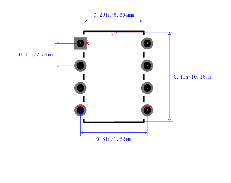
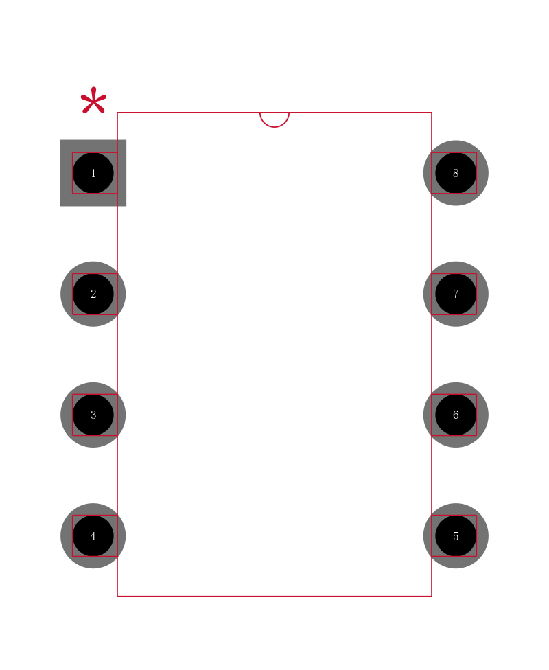
引脚数 8
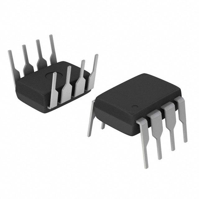
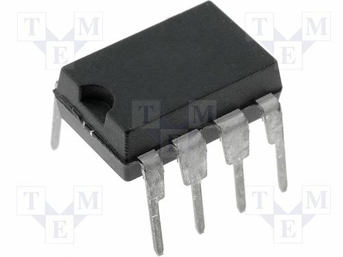
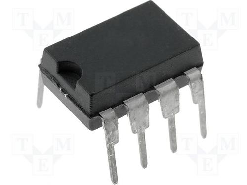
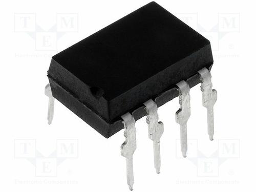
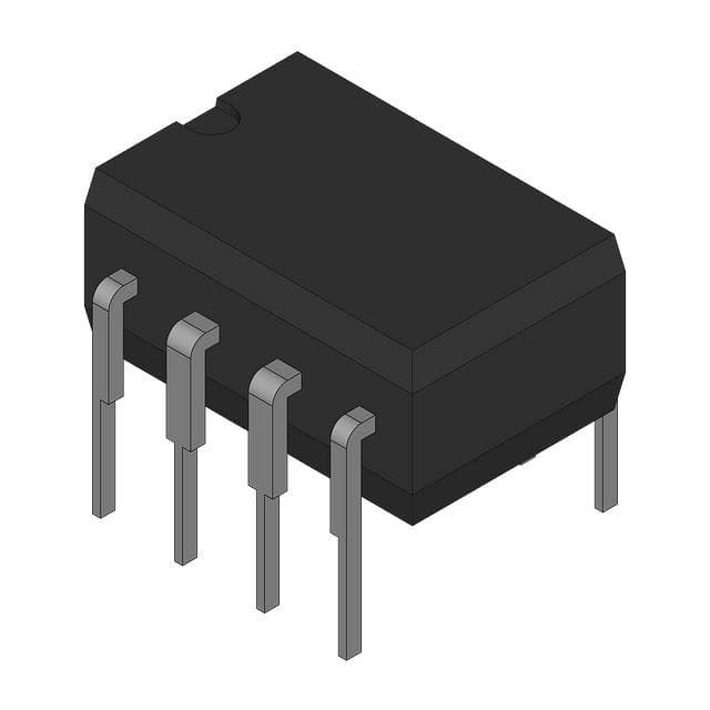
封装 PDIP-8
长度 9.81 mm
宽度 6.35 mm
高度 4.57 mm
封装 PDIP-8
工作温度 -40℃ ~ 125℃
产品生命周期 Active
包装方式 Tube
RoHS标准 RoHS Compliant
含铅标准 Lead Free
REACH SVHC版本 2015/06/15
| 型号/品牌 | 代替类型 | 替代型号对比 |
|---|---|---|
TLV2462IP TI 德州仪器 | 当前型号 | 当前型号 |
TLV2462CP 德州仪器 | 类似代替 | TLV2462IP和TLV2462CP的区别 |
TLV2462CPE4 德州仪器 | 类似代替 | TLV2462IP和TLV2462CPE4的区别 |
TLV2462IPE4 德州仪器 | 类似代替 | TLV2462IP和TLV2462IPE4的区别 |