


LinCMOSE低电压高速运算放大器 LinCMOSE LOW-VOLTAGE HIGH-SPEED OPERATIONAL AMPLIFIERS
The TLV234x operational amplifiers are in a family of devices that has been specifically designed for use in low-voltage single-supply applications. Unlike other products in this family designed primarily to meet aggressive power consumption specifications, the TLV234x was developed to offer ac performance approaching that of a BiFET operational amplifier while operating from a single-supply rail. At 3 V, the TLV234x has a typical slew rate of 2.1 V/us and 790-kHz unity-gain bandwidth.
Each amplifier is fully functional down to a minimum supply voltage of 2 V and is fully characterized, tested, and specified at both 3-V and 5-V power supplies over a temperature range of -40°C to 85°C. The common-mode input voltage range includes the negative rail and extends to within 1 V of the positive rail.
Low-voltage and low-power operation has been made possible by using the Texas Instruments silicon-gate LinCMOS technology. The LinCMOS process also features extremely high input impedance and ultra-low input bias currents. These parameters combined with good ac performance make the TLV234x effectual in applications such as high-frequency filters and wide-bandwidth sensors.
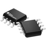
To facilitate the design of small portable equipment, the TLV234x is made available in a wide range of package options, including the small-outline and thin-shrink small-outline packages TSSOP. The TSSOP package has significantly reduced dimensions compared to a standard surface-mount package. Its maximum height of only 1.1 mm makes it particularly attractive when space is critical.
The device inputs and outputs are designed to withstand -100-mA currents without sustaining latch-up. The TLV234x incorporates internal ESD-protection circuits that prevents functional failures at voltages up to 2000 V as tested under MIL-PRF-38535, Method 3015.2; however, care should be exercised in handling these devices as exposure to ESD may result in the degradation of the device parametric performance. View datasheet View product folder
供电电流 1.4 mA
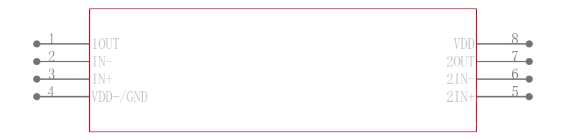
电路数 2
通道数 2
耗散功率 725 mW
共模抑制比 65 dB
输入补偿漂移 2.70 µV/K
带宽 790 kHz
转换速率 3.60 V/μs
增益频宽积 1.7 MHz
输入补偿电压 1.1 mV
输入偏置电流 0.6 pA
工作温度Max 85 ℃
工作温度Min -40 ℃
增益带宽 1.7 MHz
耗散功率Max 725 mW
共模抑制比Min 65 dB
安装方式 Surface Mount
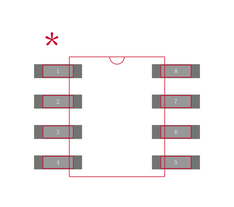
引脚数 8
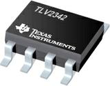
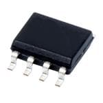
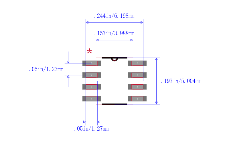
封装 SOIC-8
长度 4.9 mm
宽度 3.91 mm
高度 1.58 mm
封装 SOIC-8
工作温度 -40℃ ~ 85℃
产品生命周期 Active
包装方式 Tube
RoHS标准 RoHS Compliant
含铅标准 Lead Free
| 型号/品牌 | 代替类型 | 替代型号对比 |
|---|---|---|
TLV2342ID TI 德州仪器 | 当前型号 | 当前型号 |
TLV2342IDR 德州仪器 | 类似代替 | TLV2342ID和TLV2342IDR的区别 |
TLV2342IDRG4 德州仪器 | 类似代替 | TLV2342ID和TLV2342IDRG4的区别 |