


LinCMOSE四路运算放大器 LinCMOSE QUAD OPERATIONAL AMPLIFIERS
The TLC254, TLC254A, TLC254B, TLC25L4, TLC254L4A, TLC254L4B, TLC25M4, TLC25M4A and TL25M4B are low-cost, low-power quad operational amplifiers designed to operate with single or dual supplies. These devices utilize the Texas Instruments silicon gate LinCMOSTM process, giving them stable input-offset voltages that are available in selected grades of 2, 5, or 10 mV maximum, very high input impedances, and extremely low input offset and bias currents. Because the input common-mode range extends to the negative rail and the power consumption is extremely low, this series is ideally suited for battery-powered or energy-conserving applications. The series offers operation down to a 1.4-V supply, is stable at unity gain, and has excellent noise characteristics.
These devices have internal electrostatic-discharge ESD protection circuits that prevent catastrophic failures at voltages up to 2000 V as tested under MIL-STD-883C, Method 3015.1. However, care should be exercised in handling these devices as exposure to ESD may result in degradation of the device parametric performance.
Because of the extremely high input impedance and low input bias and offset currents, applications for these devices include many areas that have previously been limited to BIFET and NFET product types. Any circuit using high-impedance elements and requiring small offset errors is a good candidate for cost-effective use of these devices. Many features associated with bipolar technology are available with LinCMOS operational amplifiers without the power penalties of traditional bipolar devices.
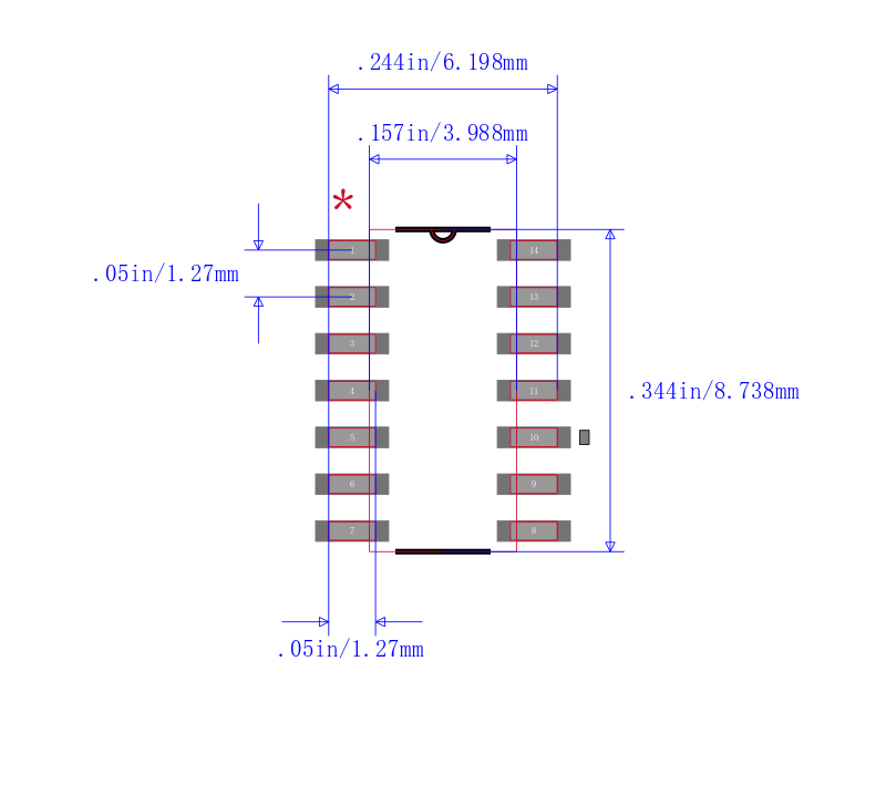
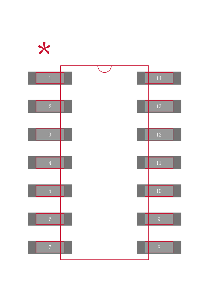
General applications such as transducer interfacing, analog calculations, amplifier blocks, active filters, and signal buffering are all easily designed with these devices. Remote and inaccessible equipment applications are possible using their low-voltage and low-power capabilities. These devices are well suited to solve the difficult problems associated with single-battery and solar-cell-powered applications. This series includes devices that are characterized for the commercial temperature range and are available in 14-pin plastic dip and the small-outline packages. The device is also available in chip form.
These devices are characterized for operation from 0°C to 70°C. View datasheet View product folder
供电电流 57 µA
电路数 4
通道数 4
耗散功率 0.725 W
共模抑制比 65 dB
输入补偿漂移 1.80 µV/K
带宽 85.0 kHz
转换速率 30.0 mV/μs
增益频宽积 110 kHz
输入补偿电压 1.1 mV
输入偏置电流 0.7 pA
工作温度Max 70 ℃
工作温度Min 0 ℃
增益带宽 0.085 MHz
耗散功率Max 725 mW
共模抑制比Min 65 dB
安装方式 Surface Mount
引脚数 14
封装 SOIC-14
封装 SOIC-14
工作温度 0℃ ~ 70℃
产品生命周期 Active
包装方式 Tube
RoHS标准 RoHS Compliant
含铅标准 Lead Free
| 型号/品牌 | 代替类型 | 替代型号对比 |
|---|---|---|
TLC25L4CD TI 德州仪器 | 当前型号 | 当前型号 |
TLC25L4CDG4 德州仪器 | 完全替代 | TLC25L4CD和TLC25L4CDG4的区别 |
TLC25L4CDR 德州仪器 | 类似代替 | TLC25L4CD和TLC25L4CDR的区别 |