

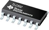

双LINCMOSE⑩定时器 DUAL LINCMOSE⑩ TIMER
The TLC552 is a dual monolithic timing circuit fabricated using LinCMOSTM process, which provides full compatibility with CMOS, TTL, and MOS logic and operation at frequencies up to 2 MHz. Accurate time delays and oscillations are possible with smaller, less-expensive timing capacitors than the NE555 because of the high input impedance. Power consumption is low across the full range of power supply voltages.
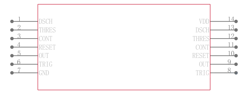
Like the NE556, the TLC552 has a trigger level approximately one-third of the supply voltage and a threshold level approximately two-thirds of the supply voltage. These levels can be altered by use of the control voltage terminal. When the trigger input falls below the trigger level, the flip-flop is set and the output goes high. If the trigger input is above the trigger level and the threshold input is above the threshold level, the flip-flop is reset and the output is low. The reset input can override all other inputs and can be used to initiate a new timing cycle. If the reset input is low, the flip-flop is reset and the output is low. Whenever the output is low, a low-impedance path is provided between the discharge terminal and ground.
While the CMOS output is capable of sinking over 100 mA and sourcing over 10 mA, the TLC552 exhibits greatly reduced supply-current spikes during output transitions. This minimizes the need for the large decoupling capacitors required by the NE556.
These devices have internal electrostatic discharge ESD protection circuits that will prevent catastrophic failures at voltages up to 2000 V as tested under MIL-STD-883C, Method 3105.2. However, care should be exercised in handling these devices as exposure to ESD may result in a degradation of the device parametric performance.
All unused inputs should be tied to an appropriate logic level to prevent false triggering.
The TLC552C is characterized for operation from 0°C to 70°C.
View datasheet View product folder
频率 2.8 MHz
电源电压DC 1.00V min
供电电流 1.6 mA
耗散功率 1.15 W
静态电流 340 µA
工作温度Max 70 ℃
工作温度Min 0 ℃
耗散功率Max 1150 mW
电源电压 1V ~ 18V
电源电压Max 18 V
电源电压Min 1 V
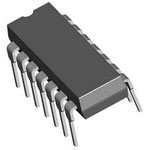
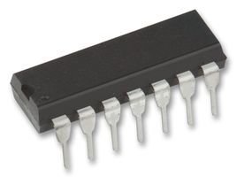
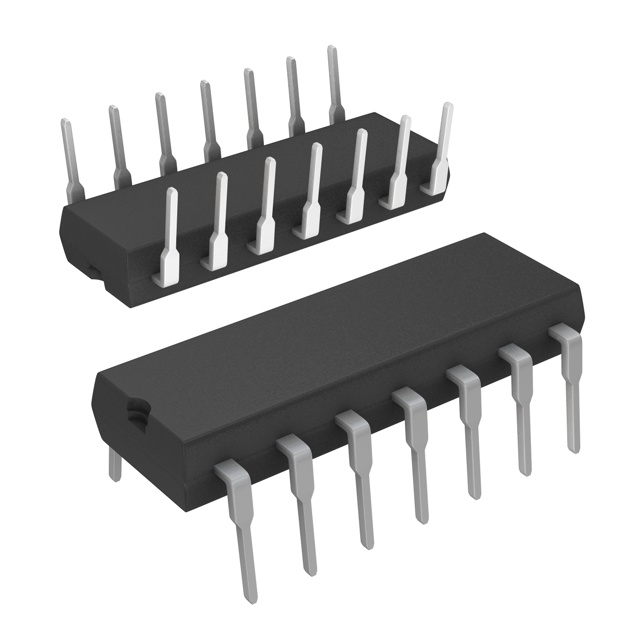
安装方式 Through Hole
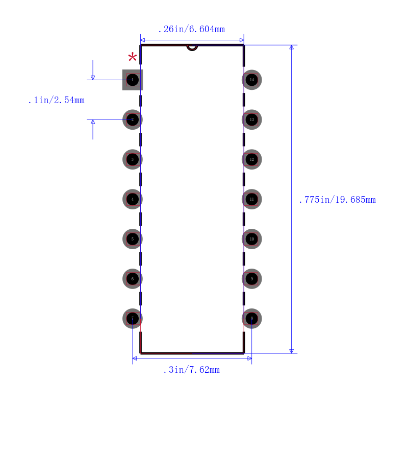
引脚数 14
封装 PDIP-14
封装 PDIP-14
工作温度 0℃ ~ 70℃
产品生命周期 Active
包装方式 Tube
RoHS标准 RoHS Compliant
含铅标准 Lead Free
REACH SVHC版本 2015/06/15
ECCN代码 EAR99

| 型号/品牌 | 代替类型 | 替代型号对比 |
|---|---|---|
TLC552CN TI 德州仪器 | 当前型号 | 当前型号 |
NE556N 德州仪器 | 类似代替 | TLC552CN和NE556N的区别 |
TLC556IN 德州仪器 | 类似代替 | TLC552CN和TLC556IN的区别 |
TLC556INE4 德州仪器 | 类似代替 | TLC552CN和TLC556INE4的区别 |