


LINEPIC,自校准精密运放
description
The TLC4501 and TLC4502 are the highest precision CMOS single supply rail-to-rail operational amplifiers available today. The input offset voltage is 10 µV typical and 40 µV maximum. This exceptional precision, combined with a 4.7-MHz bandwidth, 2.5-V/µs slew rate, and 50-mA output drive, is ideal for multiple applications including: data acquisition systems, measurement equipment, industrial control applications, and portable digital scales.
Self-Calibrates Input Offset Voltage to 40 µV Max
Low Input Offset Voltage Drift . . . 1 µV/°C
Input Bias Current . . . 1 pA
Open Loop Gain . . . 120 dB
Rail-To-Rail Output Voltage Swing
Stable Driving 1000 pF Capacitive Loads
Gain Bandwidth Product . . . 4.7 MHz
Slew Rate . . . 2.5 V/µs
High Output Drive Capability . . . ±50 mA
Calibration Time . . . 300 ms
Characterized From –55°C to 125°C
Available in Q-Temp Automotive
HighRel Automotive Applications
Configuration Control / Print Support
Qualification to Automotive Standards
输出电流 ≤100 mA
供电电流 1 mA
电路数 1
通道数 1
耗散功率 0.725 W
共模抑制比 90 dB
输入补偿漂移 1.00 µV/K
带宽 4.70 MHz
转换速率 2.50 V/μs
增益频宽积 4.7 MHz
输入补偿电压 10 µV
输入偏置电流 1 pA
工作温度Max 70 ℃
工作温度Min 0 ℃
增益带宽 4.7 MHz
耗散功率Max 725 mW
共模抑制比Min 90 dB
安装方式 Surface Mount
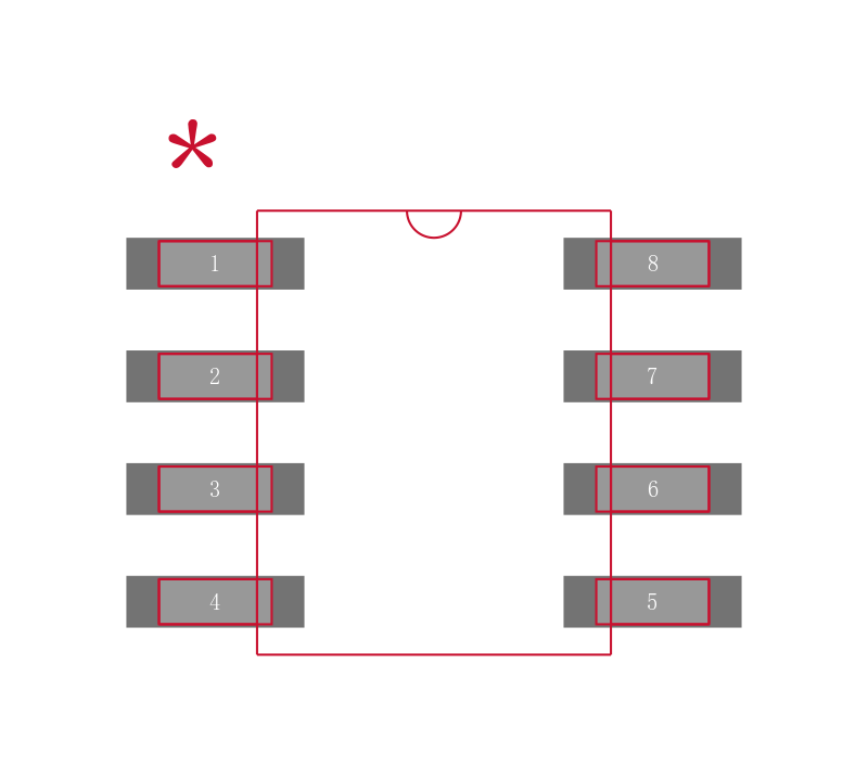
引脚数 8
封装 SOIC-8
封装 SOIC-8
工作温度 0℃ ~ 70℃
产品生命周期 Active
包装方式 Tube
RoHS标准 RoHS Compliant
含铅标准 Lead Free

| 型号/品牌 | 代替类型 | 替代型号对比 |
|---|---|---|
TLC4501CD TI 德州仪器 | 当前型号 | 当前型号 |
LMP2011MA/NOPB 德州仪器 | 类似代替 | TLC4501CD和LMP2011MA/NOPB的区别 |
TLC4501ACD 德州仪器 | 类似代替 | TLC4501CD和TLC4501ACD的区别 |
OPA335AIDR 德州仪器 | 类似代替 | TLC4501CD和OPA335AIDR的区别 |