带自动流控异步通信部件 ASYNCHRONOUS COMMUNICATIONS ELEMENT WITH AUTOFLOW CONTROL
DESCRIPON
The TL16C550D and the TL16C550DI are speed and operating voltage upgrades but functional equivalents of the TL16C550C asynchronous communications element ACE, which in turn is a functional upgrade of the TL16C450. Functionally equivalent to the TL16C450 on power up character or TL16C450 mode,
艾睿:
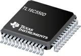
UART 1-CH 16Byte FIFO 2.5V/3.3V/5V 48-Pin TQFP T/R
安富利:
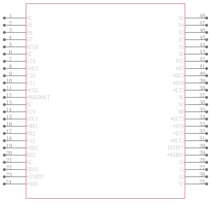
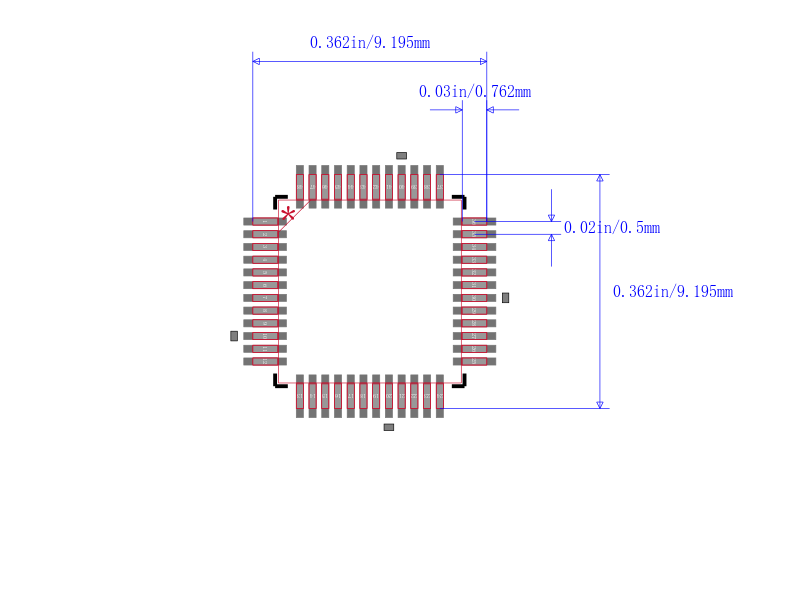
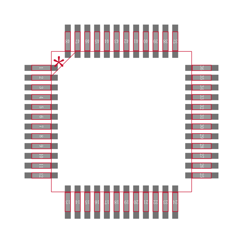
The TL16C550D and the TL16C550DI are speed and operating voltage upgrades but functional equivalents of the TL16C550C asynchronous communications element ACE, which in turn is a functional upgrade of the TL16C450. Functionally equivalent to the TL16C450 on power up character or TL16C450 mode, the TL16C550D and the TL16C550DI, like the TL16C550C, can be placed in an alternate FIFO mode. This relieves the CPU of excessive software overhead by buffering received and transmitted characters. The receiver and transmitter FIFOs store up to 16 bytes including three additional bits of error status per byte for the receiver FIFO. In the FIFO mode, there is a selectable autoflow control feature that can significantly reduce software overload and increase system efficiency by automatically controlling serial data flow using RTS\ output and CTS\ input signals.The TL16C550D and TL16C550DI perform serial-to-parallel conversions on data received from a peripheral device or modem and parallel-to-serial conversion on data received from its CPU. The CPU can read the ACE status at any time. The ACE includes complete modem control capability and a processor interrupt system that can be tailored to minimize software management of the communications link.Both the TL16C550D and the TL16C550DI ACE include a programmable baud rate generator capable of dividing a reference clock by divisors from 1 to 65535 and producing a 16× reference clock for the internal transmitter logic. Provisions are included to use this 16× clock for the receiver logic. The ACE accommodates up to a 1.5-Mbaud serial rate 24-MHz input clock so that a bit time is 667 ns and a typical character time is 6.7 ms start bit, 8 data bits, stop bit. Two of the TL16C450 terminal functions on the TL16C550D and the TL16C550DI have been changed to TXRDY\ and RXRDY\ , which provide signaling to a DMA controller.The TL16C550D is being made available in a reduced pin count package, the 32-pin RHB package. This is accomplished by eliminating some signals that are not required for some applications. These include the CS0, CS1, ADS\ , RD2, WR2, and RCLK input signals and the DDIS, TXRDY\ , RXRDY\ , OUT1\ , OUT2\ , and BAUDOUT\ output signals. There is an internal connection between BAUDOUT\ and RCLK. All of the functionality of the TL16C550D is maintained in the RHB package.The TL16C550D is being made available in a reduced pin count package, the 24-pin ZQS package. This is accomplished by eliminating some signals that are not required for some applications. These include the CS0, CS1, ADS\ , RD2, WR2, DSR\ , RI\ , DCD\ , and RCLK input signals and the DDIS, TXRDY\ , RXRDY\ , OUT1\ , OUT2\ , DTR\ , and BAUDOUT\ output signals. There is an internal connection between BAUDOUT\ and RCLK. Most of the functionality of the TL16C550D is maintained in the ZQS package, except that which involves the eliminated signals.
Chip1Stop:
UART 1-CH 16Byte FIFO 2.5V/3.3V/5V 48-Pin TQFP T/R
Verical:
UART 1-CH 16byte FIFO 2.5V/3.3V/5V 48-Pin TQFP T/R
| 型号/品牌 | 代替类型 | 替代型号对比 |
|---|---|---|
TL16C550DIPFBRG4 TI 德州仪器 | 当前型号 | 当前型号 |
TL16C550DIPFB 德州仪器 | 完全替代 | TL16C550DIPFBRG4和TL16C550DIPFB的区别 |
TL16C2550IPFB 德州仪器 | 类似代替 | TL16C550DIPFBRG4和TL16C2550IPFB的区别 |
TL16C550CFN 德州仪器 | 功能相似 | TL16C550DIPFBRG4和TL16C550CFN的区别 |