


D/A转换器
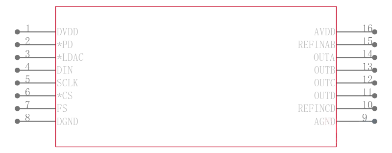
The TLV5614 is a quadruple 12-bit voltage output digital-to-analog converter DAC with a flexible 4-wire serial interface. The 4-wire serial interface allows glueless interface to TMS320, SPI, QSPI, and Microwire serial ports. The TLV5614 is programmed with a 16-bit serial word comprised of a DAC address, individual DAC control bits, and a 12-bit DAC value. The device has provision for two supplies: one digital supply for the serial interface via pins DVDD and DGND, and one for the DACs, reference buffers, and output buffers via pins AVDD and AGND. Each supply is independent of the other, and can be any value between 2.7 V and 5.5 V. The dual supplies allow a typical application where the DAC will be controlled via a microprocessor operating on a 3 V supply also used on pins DVDD and DGND, with the DACs operating on a 5 V supply. Of course, the digital and analog supplies can be tied together.
The resistor string output voltage is buffered by a x2 gain rail-to-rail output buffer. The buffer features a Class AB output stage to improve stability and reduce settling time. A rail-to-rail output stage and a power-down mode makes it ideal for single voltage, battery based applications. The settling time of the DAC is programmable to allow the designer to optimize speed versus power dissipation. The settling time is chosen by the control bits within the 16-bit serial input string. A high-impedance buffer is integrated on the REFINAB and REFINCD terminals to reduce the need for a low source impedance drive to the terminal. REFINAB and REFINCD allow DACs A and B to have a different reference voltage then DACs C and D.
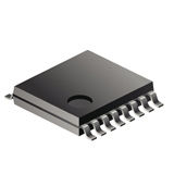
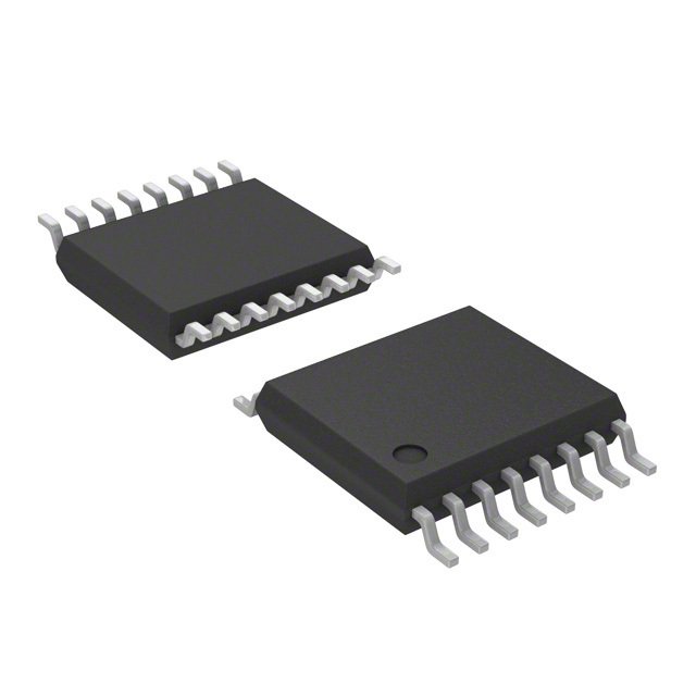
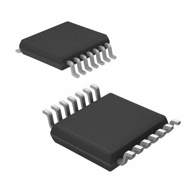
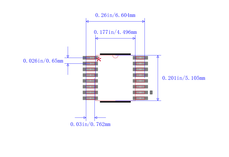
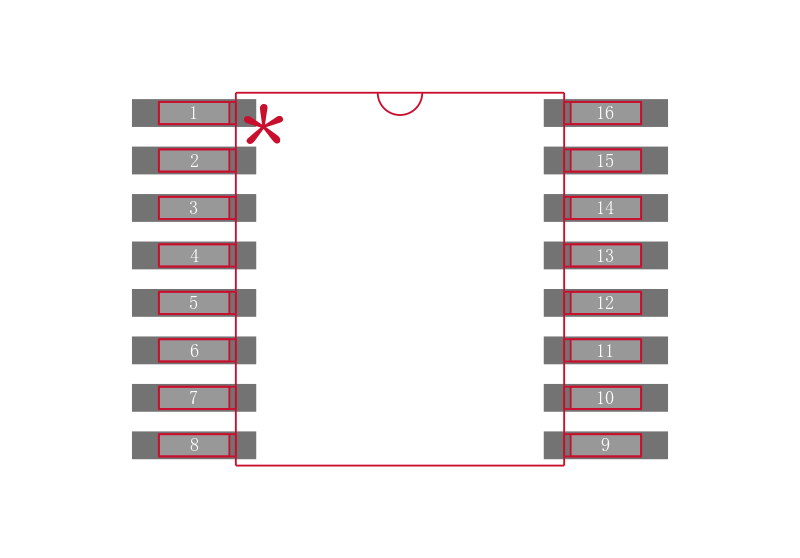
The TLV5614 is implemented with a CMOS process and is available in a 16-terminal SOIC package. The TLV5614C is characterized for operation from 0°C to 70°C. The TLV5614I is characterized for operation from 40°C to 85°C.
| 型号/品牌 | 代替类型 | 替代型号对比 |
|---|---|---|
TLV5614IPWR TI 德州仪器 | 当前型号 | 当前型号 |
TLV5614IPW 德州仪器 | 类似代替 | TLV5614IPWR和TLV5614IPW的区别 |
TLV5614CPW 德州仪器 | 类似代替 | TLV5614IPWR和TLV5614CPW的区别 |
TLV5614CPWR 德州仪器 | 类似代替 | TLV5614IPWR和TLV5614CPWR的区别 |