
TPS62065QDSGRQ1 编带
Description
The TPS62065-Q1 and TPS62067-Q1 device is a highly-efficient synchronous step-down DC-DC converter. The device provides up to 2-A output current.
With an input voltage range of 2.9 V to 6 V the device is a perfect fit for power conversion from a 5-V or 3.3-V system supply rail. The TPS62065-Q1 and TPS62067-Q1 device operates at 3-MHz fixed frequency and enters power-save mode operation at light load currents to maintain high efficiency over the entire load current range. The power save mode is optimized for low output-voltage ripple. For low noise applications, the TPS62065-Q1 device can be forced into fixed frequency PWM mode by pulling the MODE pin high. The TPS62067-Q1 provides an open drain power good output. In the shutdown mode, the current consumption is reduced to 5 µA and an internal circuit discharges the output capacitor. The TPS62065-Q1 and TPS62067-Q1 device is optimized for operation with a tiny 1-µH inductor and a small 10-µF output capacitor to achieve smallest solution size and high regulation performance.
Features
• Qualified for Automotive Applications
• AEC-Q100 Qualified With the Following Results:
– Device Temperature Grade 1: –40°C to 125°C Operating Junction Temperature Range
– Device HBM ESD Classification Level 2
– Device CDM ESD Classification Level C4B
• 3-MHz Switching Frequency
• VIN Range from 2.9 V to 6 V
• Up to 97% Efficiency
• Power Save Mode and 3-MHz Fixed PWM Mode
• Power Good Output
• Output Voltage Accuracy in PWM Mode ±1.5%
• Output Capacitor Discharge Function
• Typical 18-µA Quiescent Current
• 100% Duty Cycle for Lowest Dropout
• Voltage Positioning
• Clock Dithering
• Supports Maximum 1-mm Height Solutions
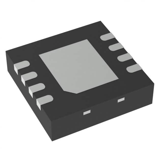
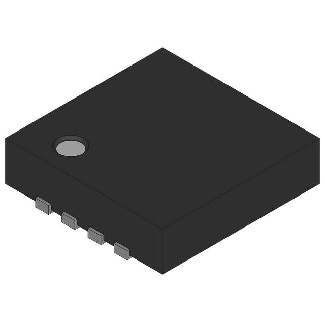
• Available in a 2 × 2 × 0,75-mm WSON
Applications
• Point Of Load Regulator
• Automotive POL
• Automotive Camera Modules
• Car Infotainment and Navigation Systems
• ADAS Applications
输出接口数 1
输出电压 0.8V ~ 6V
输出电流 2 A
静态电流 18.0 µA
调节输出数 1
开关频率 3 MHz
拓扑结构 Buck
开关电流 2.75 A
输入电压Max 6 V
输入电压Min 2.9 V
输出电压Max 6 V
输出电压Min 0.8 V
输出电流Max 2 A
工作温度Max 125 ℃
工作温度Min -40 ℃
电源电压Min 2.9 V
输入电压 3.6 V
安装方式 Surface Mount
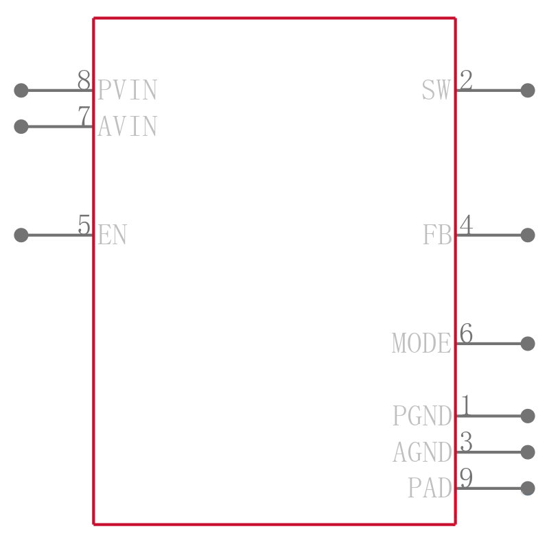
引脚数 8
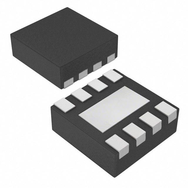
封装 WFDFN-8
长度 2 mm
宽度 2 mm
高度 0.8 mm
封装 WFDFN-8
工作温度 -40℃ ~ 125℃ TJ
产品生命周期 Active
包装方式 Tape & Reel TR
RoHS标准 RoHS Compliant
含铅标准 Lead Free
ECCN代码 EAR99