


2.7 V至5.5 V 12位并行数字 - 模拟与POWER DOWN转换器 2.7 V TO 5.5 V 12-BIT PARALLEL DIGITAL-TO-ANALOG CONVERTER WITH POWER DOWN
DESCRIPON
The TLV5619 is a 12-bit voltage output DAC with a microprocessor and TMS320 compatible parallel interface. The 12 data bits are double buffered so that the output can be updated asynchronously using the LDAC pin. During normal operation, the device dissi-pates 8 mW at a 5-V supply and 4.3 mW at a 3-V supply. The power consumption can be lowered to 50 nW by setting the DAC to power-down mode.
The output voltage is buffered by a ×2 gain rail-to-rail amplifier, which features a Class A output stage to improve stability and reduce settling time.
FEATURES
• Single Supply 2.7-V to 5.5-V Operation
• ± 0.4 LSB Differential Nonlinearity DNL,
±1.5 LSB Integral Nonlinearity INL
• 12-Bit Parallel Interface
• Compatible With TMS320 DSP
• Internal Power On Reset
• Settling Time 1 µs Typ
• Low Power Consumption:
– 8 mW for 5-V Supply
– 4.3 mW for 3-V Supply
• Reference Input Buffers
• Voltage Output
• Monotonic Over Temperature
• Asynchronous Update
APPLICATIONS
• Battery Powered Test Instruments
• Digital Offset and Gain Adjustment
• Battery Operated/Remote Industrial Controls
• Machine and Motion Control Devices
• Cordless and Wireless Telephones
• Speech Synthesis
• Communication Modulators
• Arbitrary Waveform Generation
电源电压DC 7.00 V
输出电压 400 mV
供电电流 1.60 mA
通道数 1
位数 12
采样率 480 ksps
功耗 4.30 mW
过温保护 No
工作温度Max 85 ℃
工作温度Min 40 ℃
耗散功率Max 8 mW
数模转换数DAC 1
电源电压Max 5.5 V
电源电压Min 2.7 V
安装方式 Surface Mount
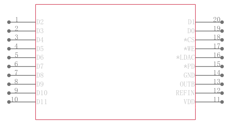
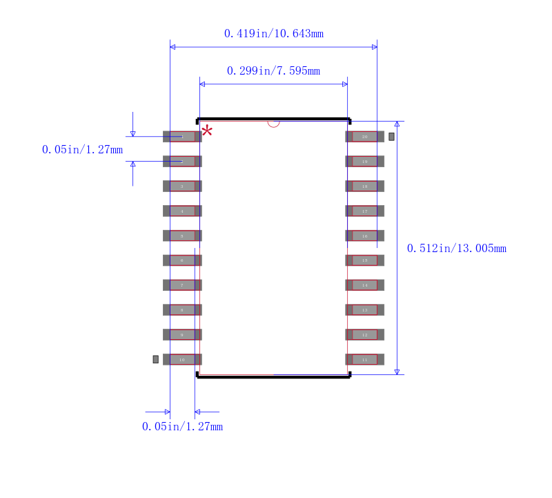
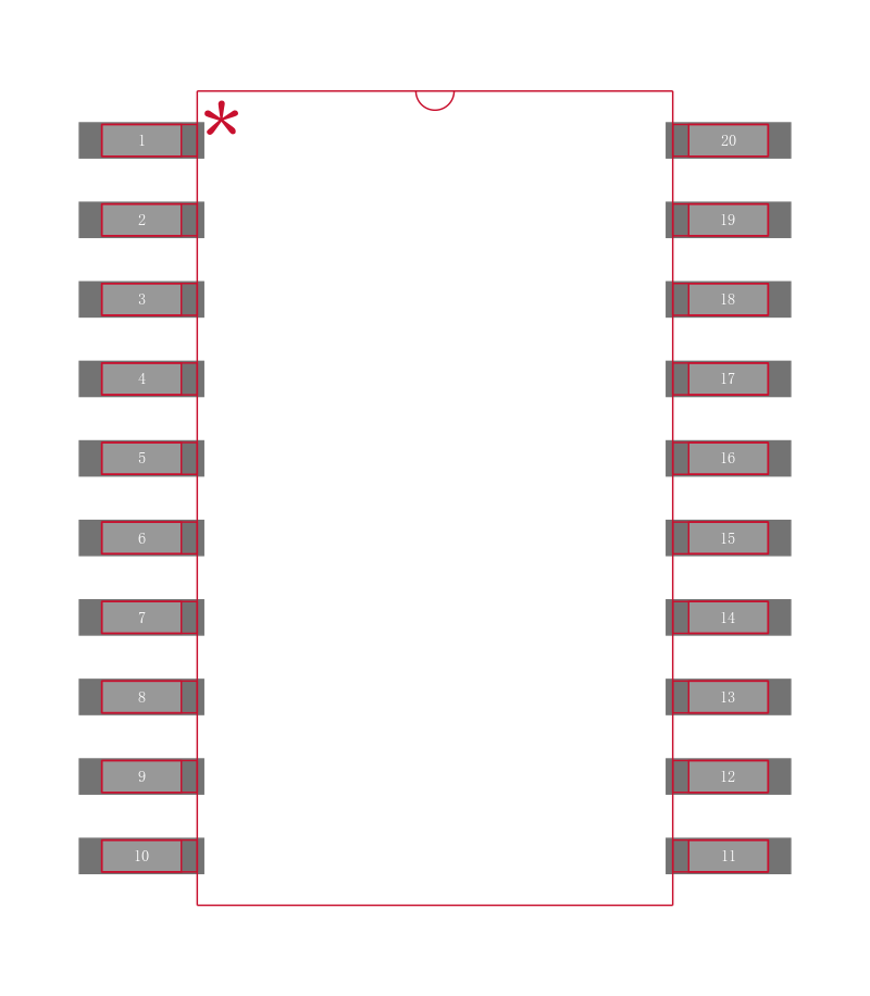
引脚数 20
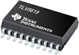
封装 SOIC-20
高度 2.35 mm
封装 SOIC-20
工作温度 -40℃ ~ 125℃
产品生命周期 Obsolete
包装方式 Tube
RoHS标准 RoHS Compliant
含铅标准 Lead Free
| 型号/品牌 | 代替类型 | 替代型号对比 |
|---|---|---|
TLV5619QDW TI 德州仪器 | 当前型号 | 当前型号 |
TLV5619CDW 德州仪器 | 完全替代 | TLV5619QDW和TLV5619CDW的区别 |
TLV5619IDW 德州仪器 | 类似代替 | TLV5619QDW和TLV5619IDW的区别 |
TLV5619QDWREP 德州仪器 | 类似代替 | TLV5619QDW和TLV5619QDWREP的区别 |