路LinCMOS可编程低功耗TIONAL放大器 LinCMOS PROGRAMMABLE LOW-POWER TIONAL AMPLIFIERS
description
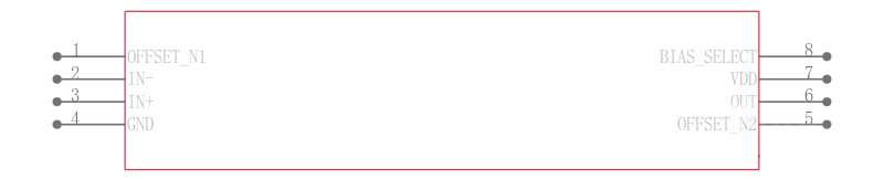
The TLC271 operational amplifier combines a wide range of input offset voltage grades with low offset voltage drift and high input impedance. In addition, the TLC271 offers a bias-select mode that allows the user to select the best combination of power dissipation and ac performance for a particular application. These devices use Texas Instruments silicon-gate LinCMOS technology, which provides offset voltage stability far exceeding the stability available with conventional metal-gate processes.
Input Offset Voltage Drift...Typically 0.1 µV/Month, Including the First 30 Days
Wide Range of Supply Voltages Over Specified Temperature Range:
0°C to 70°C...3 V to 16 V
–40°C to 85°C...4 V to 16 V
–55°C to 125°C...5 V to 16 V
Single-Supply Operation
Common-Mode Input Voltage Range Extends Below the Negative Rail C-Suffix and I-Suffix Types
Low Noise. . . 25 nV/√HzTypically at f = 1 kHz High-Bias Mode
Output Voltage Range Includes Negative Rail
High Input Impedance...1012ΩTyp
ESD-Protection Circuitry
Small-Outline Package Option Also Available in Tape and Reel
Designed-In Latch-Up Immunity