
四路低电压 LinCMOSTM 差动比较器
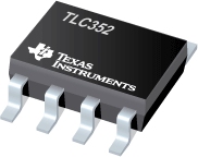
This device is fabricated using LinCMOS technology and consists of two independent voltage comparators, each designed to operate from a single power supply. Operation from dual supplies is also possible if the difference between the two supplies is 1.4 V to 18 V. Each device features extremely high input impedance typically greater than 1012 , which allows direct interface to high-impedance sources. The output are n-channel open-drain configurations and can be connected to achieve positive-logic wired-AND relationships. The capability of the to operate from 1.4-V supply makes this device ideal for low-voltage battery applications.
The TLC352 has internal electrostatic discharge ESD protection circuits and has been classified with a 2000-V ESD rating tested under MIL-STD-883C, Method 3015. However, care should be exercised in handling this device as exposure to ESD may result in degradation of the device parametric performance.
The TLC352C is characterized for operation from 0°C to 70°C. The TLC352I is characterized for operation over the industrial temperature range of 40°C to 85°C.
- .
- Single- or Dual-Supply Operation
- .
- Wide Range of Supply Voltages
1.5 V to 18 V
- .
- Very Low Supply Current Drain
150 uA Typ at 5 V
65 uA Typ at 1.4 V
- .
- Built-In ESD Protection
- .
- High Input Impedance ...1012 Typ
- .
- Extremely Low Input Bias Current 5 pA Typ
- .
- Ultrastable Low Input Offset Voltage
- .
- Input Offset Voltage Change at Worst-Case Input Conditions Typically 0.23 uV/ Month, Including the First 30 Days
- .
- Common-Mode Input Voltage Range Includes Ground
- .
- Outputs Compatible With TTL, MOS, and CMOS
- .
- Pin-Compatible With LM393
LinCMOS is a trademark of Texas Instruments Incorporated.