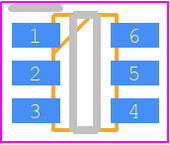

具备可调节上升和可调节输出放电的 18V、3A、79mΩ 负载开关 6-SOT-23 -40 to 105
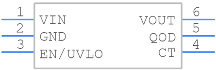
The TPS22810 is a single channel load switch with configurable rise time and with an integrated quick output discharge QOD. In addition, the device features thermal shutdown to protect the device against high junction temperature. Because of this, safe operating area of the device is inherently ensured. The device contains an N-channel MOSFET that can operate over an input voltage range of 2.7 V to 18 V. SOT23-5 DBV package can support a maximum current of 2 A. WSON DRV package can support a maximum current of 3 A. The switch is controlled by an on and off input, which is capable of interfacing directly with low-voltage control signals.
The configurable rise time of the device greatly reduces inrush current caused by large bulk load capacitances, thereby reducing or eliminating power supply droop. Undervoltage lock-out is used to turn off the device if the VIN voltage drops below a threshold value, ensuring that the downstream circuitry is not damaged by being supplied by a voltage lower than intended. The configurable QOD pin controls the fall time of the device to allow design flexibility for power down.
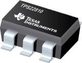
The TPS22810 is available in a leaded, SOT-23 package DBV which allows to visually inspect solder joints, as well as a WSON package DRV. The device is characterized for operation over the free-air temperature range of –40˚C to +105˚C.