

TEXAS INSTRUMENTS UCC27511DBVR 驱动器, IGBT, MOSFET, 低压侧, 4.5V-18V电源, 8A输出, -999ms 延迟, SOT-23-6
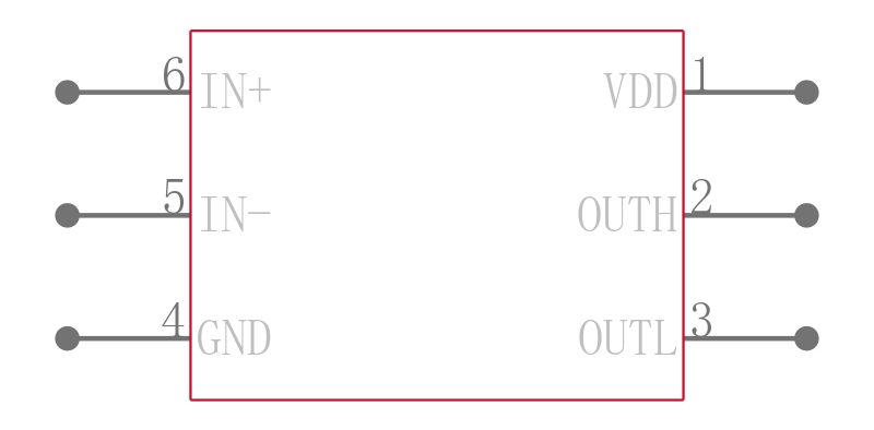
The is a 1-channel High-speed Low-side Gate Driver that can effectively drive MOSFET and IGBT power switches. Using a design that inherently minimizes shoot-through current, UCC27511 is capable of sourcing and sinking high peak-current pulses into capacitive loads offering rail-to-rail drive capability and extremely small propagation delay, typically 13ns. UCC27511 features a dual-input design which offers flexibility of implementing both inverting IN- pin and non-inverting IN+ pin configuration with the same device. Either IN+ or IN- pin can be used to control the state of the driver output. The unused input pin can be used for enable and disable functions. For safety purpose, internal pull-up and pull-down resistors on the input pins ensure that outputs are held low when input pins are in floating condition. Hence the unused input pin is not left floating and must be properly biased to ensure that driver output is in enabled for normal operation.
- .
- 4A Peak source and 8A peak sink asymmetrical drive
- .
- Strong sink current offers enhanced immunity against miller turn-on
- .
- Fast propagation delays 13ns typical
- .
- Fast rise and fall times 9ns and 7ns typical
- .
- Outputs held low during VDD UVLO
- .
- TTL and CMOS compatible input-logic threshold independent of supply voltage
- .
- Hysteretic-logic thresholds for high noise immunity
- .
- Dual-input design choice of an inverting IN- pin/non-inverting IN+ pin driver configuration
- .
- Unused input pin can be used for enable or disable function
- .
- Output held low when input pins are floating
- .
- Input pin absolute maximum voltage levels not restricted by VDD pin bias supply voltage
- .
- Green product and no Sb/Br
This device has limited built-in ESD protection, leads should be shorted together or the device placed in conductive foam during storage or handling to prevent electrostatic damage to the MOS gates.
电源电压DC 4.50V min
上升/下降时间 8ns, 7ns
输出接口数 1
针脚数 6
上升时间 22 ns
下降时间 11 ns
下降时间Max 11 ns
上升时间Max 22 ns
工作温度Max 140 ℃
工作温度Min -40 ℃
电源电压 4.5V ~ 18V
电源电压Max 18 V
电源电压Min 4.5 V
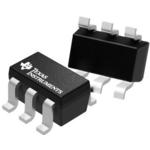
安装方式 Surface Mount
引脚数 6
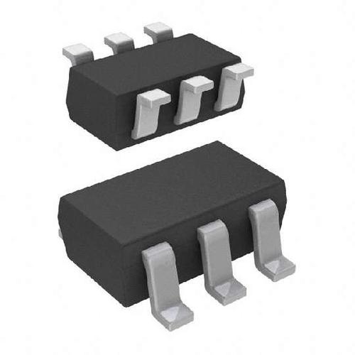
封装 SOT-23-6
封装 SOT-23-6
工作温度 -40℃ ~ 140℃
产品生命周期 Active
包装方式 Tape & Reel TR
制造应用 电机驱动与控制, 替代能源, 信号处理, 电源管理
RoHS标准 RoHS Compliant
含铅标准 Lead Free
REACH SVHC标准 No SVHC
REACH SVHC版本 2015/06/15
ECCN代码 EAR99
香港进出口证 NLR

| 型号/品牌 | 代替类型 | 替代型号对比 |
|---|---|---|
UCC27511DBVR TI 德州仪器 | 当前型号 | 当前型号 |
UCC27511DBVT 德州仪器 | 类似代替 | UCC27511DBVR和UCC27511DBVT的区别 |