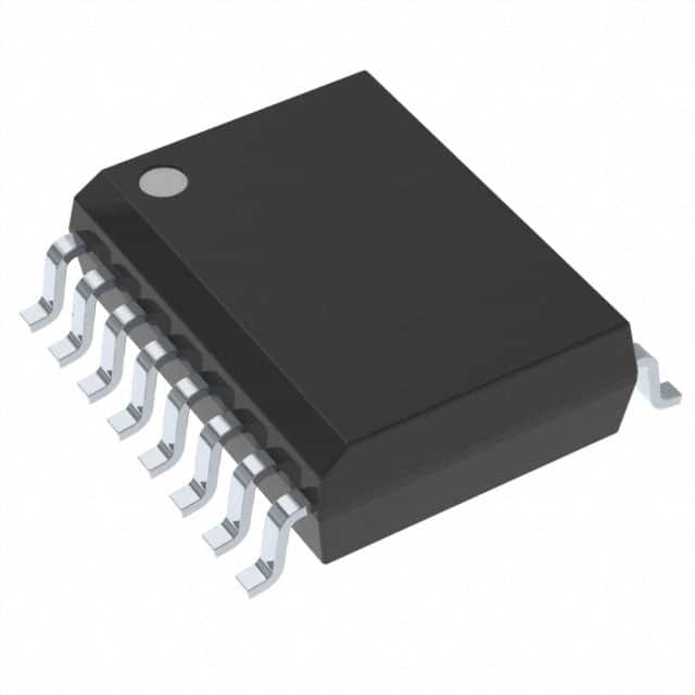
具有 8V UVLO、双输入和禁用引脚的 4A/6A、5.7kVRMS 双通道隔离式栅极驱动器 16-SOIC -40 to 125
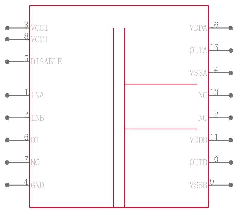
The UCC21520 is an isolated dual-channel gate driver with 4-A source and 6-A sink peak current. It is designed to drive power MOSFETs, IGBTs, and SiC MOSFETs up to 5-MHz with best-in-class propagation delay and pulse-width distortion.
The input side is isolated from the two output drivers by a 5.7-kVRMS reinforced isolation barrier, with a minimum of 100-V/ns common-mode transient immunity CM. Internal functional isolation between the two secondary-side drivers allows a working voltage of up to 1500 VDC.
This driver can be configured as two low-side drivers, two high-side drivers, or a half-bridge driver with programmable dead time DT. A disable pin shuts down both outputs simultaneously when it is set high, and allows normal operation when left open or grounded. As a fail-safe measure, primary-side logic failures force both outputs low.
The device accepts VDD supply voltages up to 25 V. A wide input VCCI range from 3 V to 18 V makes the driver suitable for interfacing with both analog and digital controllers. All the supply voltage pins have under voltage lock-out UVLO protection.
With all these advanced features, the UCC21520 enables high efficiency, high power density, and robustness in a wide variety of power applications.
上升/下降时间 6ns, 7ns
输出接口数 2
输出电压 6.5V ~ 25V
输出电流 4A, 6A
通道数 2
耗散功率 1.05 W
上升时间 6 ns
隔离电压 5700 Vrms
下降时间 7 ns
下降时间Max 12 ns
上升时间Max 16 ns
工作温度Max 125 ℃
工作温度Min -40 ℃
耗散功率Max 1050 mW
电源电压Max 18 V
电源电压Min 3 V
安装方式 Surface Mount
引脚数 16
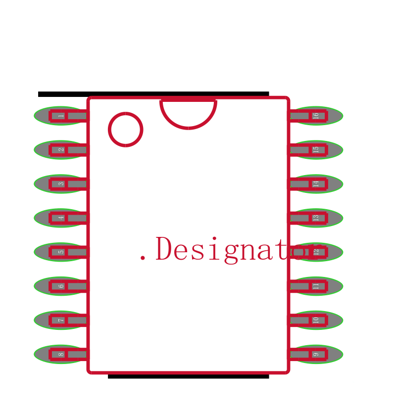
封装 SOIC-16
封装 SOIC-16
工作温度 -40℃ ~ 125℃
产品生命周期 Active
包装方式 Tube
RoHS标准 RoHS Compliant
含铅标准 无铅
ECCN代码 EAR99
| 型号/品牌 | 代替类型 | 替代型号对比 |
|---|---|---|
UCC21520ADW TI 德州仪器 | 当前型号 | 当前型号 |
UCC21520ADWR 德州仪器 | 类似代替 | UCC21520ADW和UCC21520ADWR的区别 |