
OMNIFET II完全autoprotected功率MOSFET OMNIFET II fully autoprotected Power MOSFET
Description
The VNB14NV04, VND14NV04, VND14NV04-1 and VNS14NV04 are monolithic devices made using STMicroelectronics VIPower™ M0 technology, intended for replacement of standard power MOSFETS in DC to 50 KHz applications. Built-in thermal shutdown, linear current limitation and
overvoltage clamp protect the chip in harsh environments. Fault feedback can be detected by monitoring the voltage at the input pin.
■ Linear current limitation
■ Thermal shutdown
■ Short circuit protection
■ Integrated clamp
■ Low current drawn from input pin
■ Diagnostic feedback through input pin
■ ESD protection
■ Direct access to the gate of the Power MOSFET analog driving
■ Compatible with standard Power MOSFET
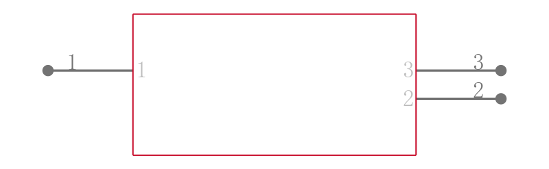
输出接口数 1
输出电流 24 A
供电电流 0.1 mA
针脚数 3
漏源极电阻 35.0 mΩ
极性 N-Channel
耗散功率 74 W
漏源击穿电压 40.0 V
连续漏极电流Ids 12.0 A
输出电流Max 12 A
输出电流Min 12 A
输入数 1
工作温度Max 150 ℃
工作温度Min -40 ℃
耗散功率Max 74000 mW
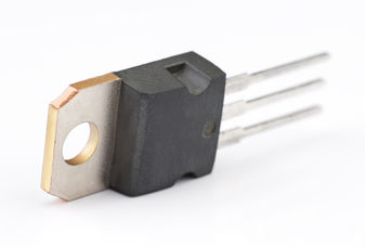
安装方式 Through Hole
引脚数 3
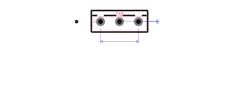
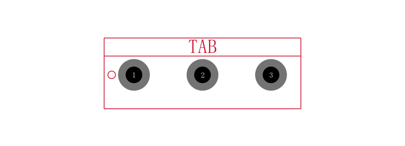
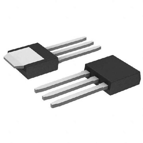
封装 TO-251-3
高度 7.2 mm
封装 TO-251-3
工作温度 -40℃ ~ 150℃ TJ
产品生命周期 Active
包装方式 Tube
RoHS标准 RoHS Compliant
含铅标准 Lead Free
ECCN代码 EAR99