


5V ECL ÷2,÷4,÷8 时钟发生芯片
The MC10/100EL34 is a low skew divide by 2, divide by 4, divide by 8 clock generation chip designed explicitly for low skew clock generation applications. The internal dividers are synchronous to each other, therefore, the common output edges are all precisely aligned. The device can be driven by either a differential or single-ended ECL or, if positive power supplies are used, PECL input signal. In addition, by using the V output, a sinusoidal source can be AC coupled into the device see Interfacing section of the ECLinPS Data Book DL140/D. If a single-ended input is to be used, the V output should be connected to the CLK input and bypassed to ground via a 0.01 F capacitor. The V output is designed to act as the switching reference for the input of the EL34 under single-ended input conditions, as a result, this pin can only source/sink up to 0.5mA of current. The common enable EN is synchronous so that the internal dividers will only be enabled/disabled when the internal clock is already in the LOW state. This avoids any chance of generating a runt clock pulse on the internal clock when the device is enabled/disabled as can happen with an asynchronous control. An internal runt pulse could lead to losing synchronization between the internal divider stages. The internal enable flip-flop is clocked on the falling edge of the input clock, therefore, all associated specification limits are referenced to the negative edge of the clock input. Upon startup, the internal flip-flops will attain a random state; the master reset MR input allows for the synchronization of the internal dividers, as well as multiple EL34s in a system.The 100 Series contains temperature compensation.
Features
---
|
- .
- 50ps Output-to-Output Skew
- .
- Synchronous Enable/Disable
- .
- Master Reset for Synchronization
- .
- PECL Mode Operating Range: VCC = 4.2 V to 5.7 V with VEE = 0 V
- .
- NECL Mode Operating Range: VCC = 0 V with VEE = -4.2 V to -5.7 V
- .
- Internal Input Pulldown Resistors on CLKs, ENbar, and MR
- .
- Pb-Free Packages are Available
频率 1.1 GHz
电源电压DC 4.20V min
无卤素状态 Halogen Free
输出接口数 3
供电电流 39.0 mA
电路数 1
工作温度Max 85 ℃
工作温度Min -40 ℃
电源电压 4.2V ~ 5.7V
电源电压Max 5.7 V
电源电压Min 4.2 V
安装方式 Surface Mount
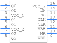
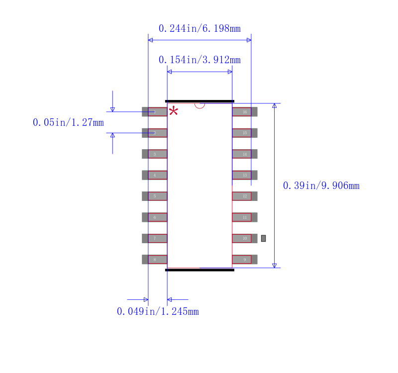
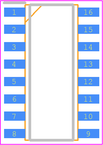
引脚数 16
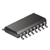
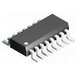
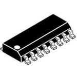
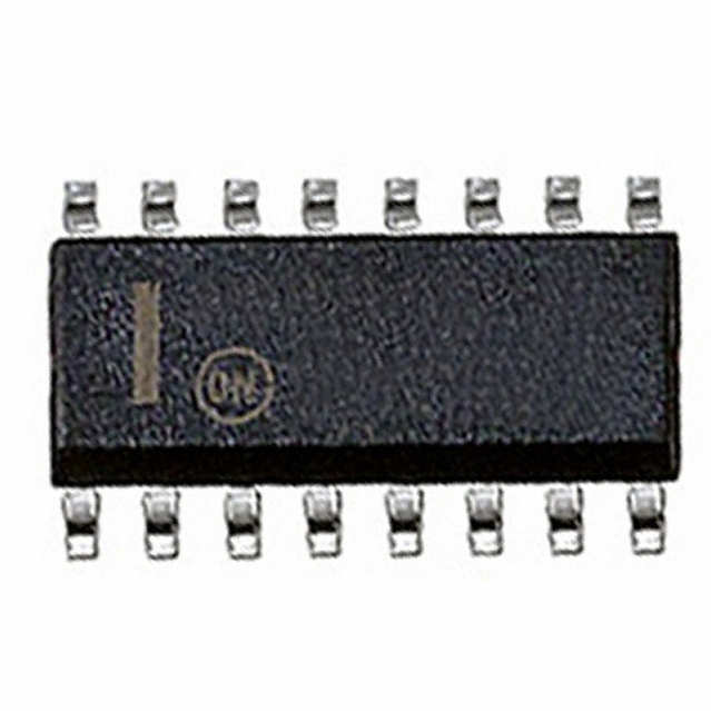
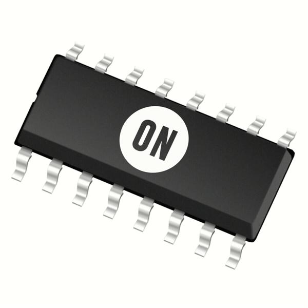
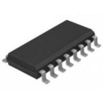
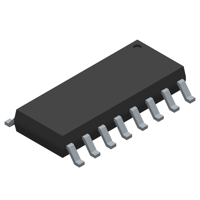
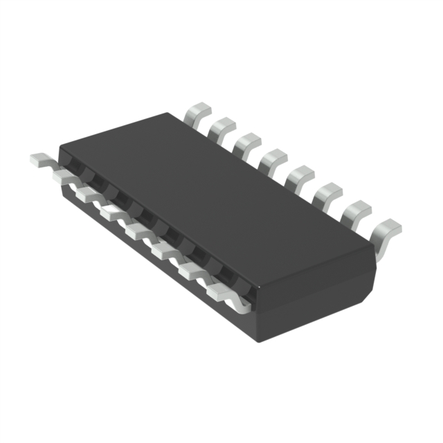
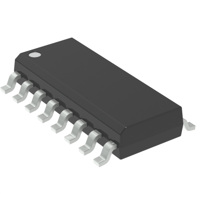
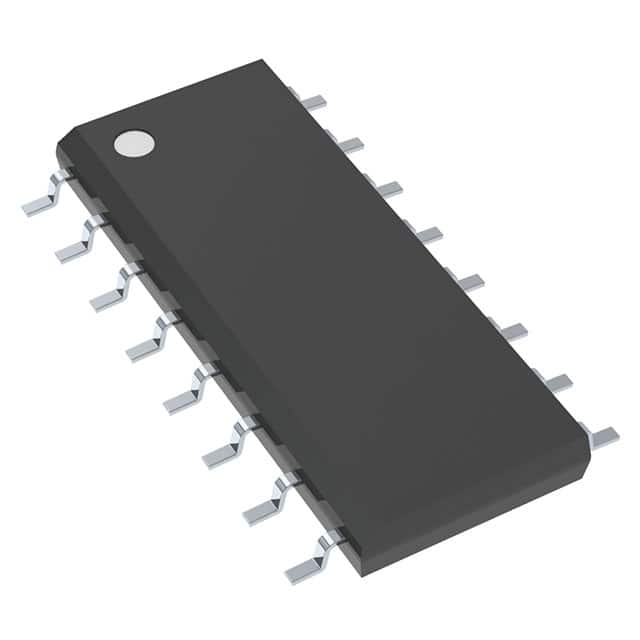
封装 SOIC-16
封装 SOIC-16
工作温度 -40℃ ~ 85℃
产品生命周期 Active
包装方式 Tube
RoHS标准 RoHS Compliant
含铅标准 Lead Free
REACH SVHC版本 2015/12/17
ECCN代码 EAR99
| 型号/品牌 | 代替类型 | 替代型号对比 |
|---|---|---|
MC100EL34DG ON Semiconductor 安森美 | 当前型号 | 当前型号 |
MC100EL34DR2G 安森美 | 完全替代 | MC100EL34DG和MC100EL34DR2G的区别 |
MC10EL34DR2G 安森美 | 完全替代 | MC100EL34DG和MC10EL34DR2G的区别 |
MC10EL34DG 安森美 | 类似代替 | MC100EL34DG和MC10EL34DG的区别 |