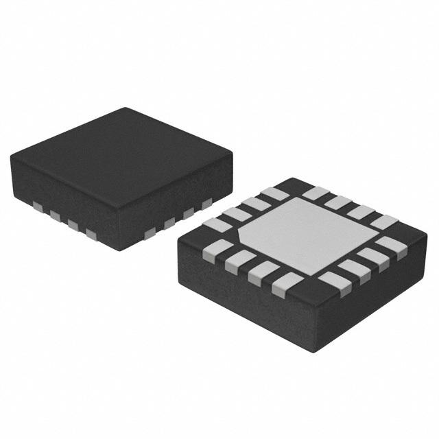

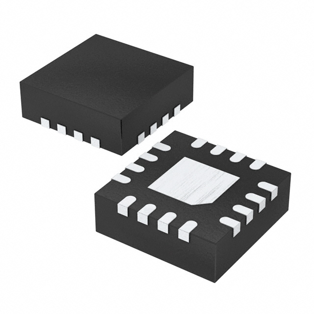


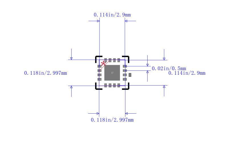
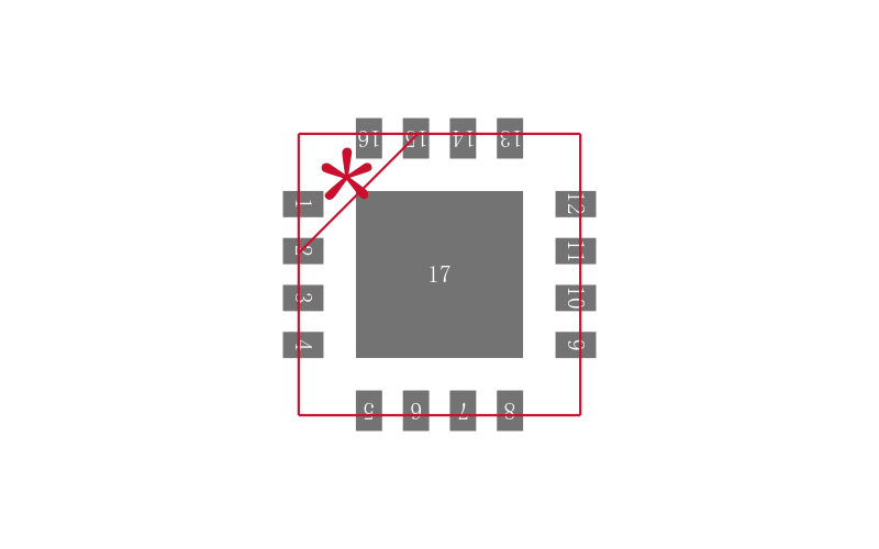
2.5V / 3.3V的SiGe差分接收器/驱动器输出RSECL 2.5V/3.3V SiGe Differential Receiver/Driver with RSECL Outputs
*Reduced Swing ECL
Description
The NBSG16 is a differential receiver/driver targeted for high frequency applications. The device is functionally equivalent to the EP16 and LVEP16 devices with much higher bandwidth and lower
EMI capabilities.
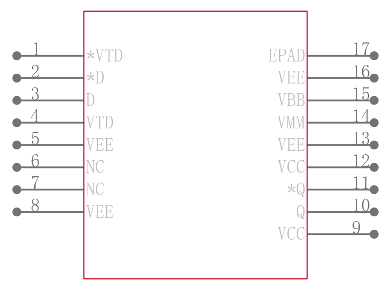
Inputs incorporate internal 50 termination resistors and accept NECL Negative ECL, PECL Positive ECL, HSTL, LVTTL, LVCMOS, CML, or LVDS. Outputs are RSECL Reduced Swing ECL, 400 mV.
Features
• Maximum Input Clock Frequency > 12 GHz Typical
• Maximum Input Data Rate > 12 Gb/s Typical
• 120 ps Typical Propagation Delay
• 40 ps Typical Rise and Fall Times
• RSPECL Output with Operating Range: VCC = 2.375 V to 3.465 V with VEE = 0 V
• RSNECL Output with RSNECL or NECL Inputs with
Operating Range: VCC = 0 V with VEE = −2.375 V to −3.465 V
• RSECL Output Level 400 mV Peak−to−Peak Output, Differential Output Only
• 50 Internal Input Termination Resistors
• Compatible with Existing 2.5 V/3.3 V LVEP, EP, and LVEL Devices
• VBB and VMM Reference Voltage Output
• Pb−Free Packages are Available
| 型号/品牌 | 代替类型 | 替代型号对比 |
|---|---|---|
NBSG16MNR2G ON Semiconductor 安森美 | 当前型号 | 当前型号 |
NBSG16MN 安森美 | 完全替代 | NBSG16MNR2G和NBSG16MN的区别 |
NBSG16MMNG 安森美 | 类似代替 | NBSG16MNR2G和NBSG16MMNG的区别 |
NBSG16MNG 安森美 | 类似代替 | NBSG16MNR2G和NBSG16MNG的区别 |