
输入/输出扩展, 8bit, 400 kHz, I2C, SMBus, 1.1 V, 3.6 V, HVQFN
Overview
The PCA9574 is a CMOS device that provides 8 bits of General Purpose parallel Input/Output GPIO expansion in low voltage processor and handheld battery powered mobile applications and was developed to enhance the family of I²C-bus I/O expanders. The improvements include lower supply current, lower operating voltage of 1.1 V to 3.6 V, dual and separate supply rails to allow voltage level translation anywhere between 1.1 V and 3.6 V, 400 kHz clock frequency, and smaller packaging. Any of the eight I/O ports can be configured as an input or output independent of each other and default on start-up to inputs. I/O expanders provide a simple solution when additional I/Os are needed while keeping interconnections to a minimum; for example in battery powered mobile applications and clamshell devices for interfacing to sensors, push buttons, keypad, etc. In addition to providing a flexible set of GPIOs, it simplifies interconnection of a processor running at one voltage level to I/O devices operating at a different usually higher voltage level. PCA9574 has built-in level shifting feature that makes these devices extremely flexible in mixed signal environments where communication between incompatible I/Os is required. The core of PCA9574 can operate at a voltage as low as 1.1 V while the I/O bank can operate in the range 1.1 V to 3.6 V. Bus-hold with programmable on-chip pull-up or pull-down feature for I/Os is also provided.
The system master can enable the I/Os as either inputs or outputs by writing to the I/O configuration register bits. The data for each input or output is kept in the corresponding Input or Output register. The polarity of the read register can be inverted with the Polarity inversion register active HIGH or active LOW operation. Either a bus-hold function or pull-up/pull-down feature can be selected by programming corresponding registers. The bus-hold provides a valid logic level when the I/O bus is not actively driven. When bus-hold feature is not selected, the I/O ports can be configured to have pull-up or pull-down by programming the pull-up/pull-down configuration register.
An open-drain interrupt output pin INT allows monitoring of the input pins and is asserted each time a change occurs on an input port unless that port is masked default = masked. A ‘GPIO All Call’ command allows programming multiple PCA9574s at the same time even if they have different individual I²C-bus addresses. This allows optimal code programming when more than one device needs to be programmed with the same instruction or if all outputs need to be turned on or off at the same time. The internal Power-On Reset POR or hardware reset pin RESET initializes the eight I/Os as inputs, sets the registers to their default values and initializes the device state machine. The I/O bank is held in its default state when the logic supply VDD is off.
One address select pin allows up to two PCA9574 devices to be connected with two different addresses on the same I²C-bus.
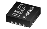
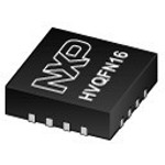
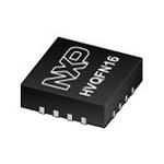
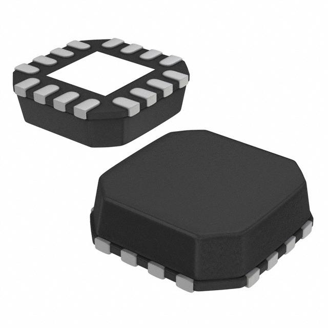
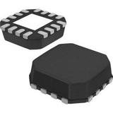
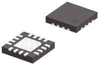
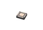
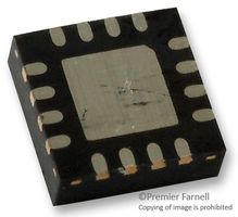
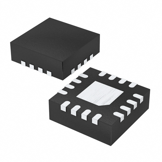
The PCA9574 is available in TSSOP16 and HVQFN16 packages and is specified over the −40 °C to +85 °C industrial temperature range.
MoreLess
## Features
* 400 kHz I²C-bus serial interface
* Compliant with I²C-bus Standard-mode 100 kHz
* Separate supply rails for core logic and I/O bank provides voltage level shifting
* 1.1 V to 3.6 V operation with level shifting feature
* Very low standby current: < 1 µA
* 8 configurable I/O pins that default to inputs at power-up
* Outputs:
* Totem pole: 1 mA source and 3 mA sink
* Independently programmable 100 kΩ pull-up or pull-down for each I/O pin
* Open-drain active LOW interrupt INT output pin allows monitoring of logic level change of pins programmed as inputs
* Inputs:
* Programmable bus hold provides valid logic level when inputs are not actively driven
* Programmable Interrupt Mask Control for input pins that do not require an interrupt when their states change or to prevent spurious interrupts default to mask at power-up
* Polarity inversion register allows inversion of the polarity of the I/O pins when read
* Active LOW reset RESET input pin resets device to power-up default state
* GPIO All Call address allows programming of more than one device at the same time with the same parameters
* 2 programmable slave addresses using 1 address pin
* -40 °C to +85 °C operation
* ESD protection exceeds 7000 V HBM per JESD22-A114 and 1000 V CDM per JESD22-C101
* Latch-up testing is done to JEDEC Standard JESD78 which exceeds 100 mA
* Packages offered: TSSOP16 and HVQFN16
## Target Applications
* Cell phones
* Media players
* Multi voltage environments
* Battery operated mobile gadgets
* Motherboards
* Servers
* RAID systems
* Industrial control
* Medical equipment
* PLCs
* Gaming machines
* Instrumentation and test measurement
## Features