8位MCU , 3.8〜 5.5 V的工作范围8〜 32 Kbyte闪存/ ROM , 10位ADC , 4个定时器, SPI , SCI 8-bit MCU, 3.8 to 5.5 V operating range with 8 to 32 Kbyte Flash/ROM, 10-bit ADC, 4 timers, SPI, SCI
The ST72324Bxx devices are members of the ST7 microcontroller family designed for midrange applications running from 3.8 to 5.5 V. Different package options offer up to 32 I/O pins.
All devices are based on a common industry-standard 8-bit core, featuring an enhanced instruction set and are available with Flash or ROM program memory. The ST7 family architecture offers both power and flexibility to software developers, enabling the design of highly efficient and compact application code.
The on-chip peripherals include an A/D converter, two general purpose timers, an SPI interface and an SCI interface. For power economy, the microcontroller can switch dynamically into, Slow, Wait, Active-halt or Halt mode when the application is in idle or stand-by state.
Typical applications include consumer, home, office and industrial products.
**Key Features**
- .
- 1 analog peripheral low current coupling10-bit ADC with up to 12 input ports
- .
- 2 communication interfacesSPI synchronous serial interfaceSCI asynchronous serial interface
- .
- Memories8 to 32 Kbyte dual voltage High Density Flash HDFlash or ROM with readout protection capability. In-application programming and Incircuit programming for HDFlash devices384 bytes to 1 Kbyte RAMHDFlash endurance: 1 kcycle at 55 °C, data retention 40 years at 85 °C
- .
- Interrupt managementNested interrupt controller. 10 interrupt vectors plus TRAP and RESET. 9/6 ext. interrupt lines on 4 vectors
- .
- Clock, reset and supply managementEnhanced low voltage supervisor LVD with programmable reset thresholds and auxiliary voltage detector AVD with interrupt capabilityClock sources: crystal/ceramic resonator oscillators, int. RC osc. and ext. clock inputPLL for 2x frequency multiplication4 power saving modes: Slow, Wait, Active-halt, and Halt
- .
- 4 timersMain clock controller with real-time base, Beep and clock-out capabilitiesConfigurable watchdog timer16-bit Timer A with 1 input capture, 1 output compare, ext. clock input, PWM and pulse generator modes16-bit Timer B with 2 input captures, 2 output compares, PWM and pulse generator modes
- .
- Development toolsIn-circuit testing capability
- .
- Up to 32 I/O ports32/24 multifunctional bidirectional I/Os, 22/17 alternate function lines, 12/10 high sink outputs
频率 8 MHz
电源电压DC 5.00 V, 5.50 V max
时钟频率 8.00 MHz, 8.00 MHz max
RAM大小 384 x 8
I/O引脚数 32
存取时间 8.00 µs
工作温度Max 85 ℃
工作温度Min -40 ℃
耗散功率Max 500 mW
电源电压Max 5.5 V
电源电压Min 3.8 V
安装方式 Surface Mount
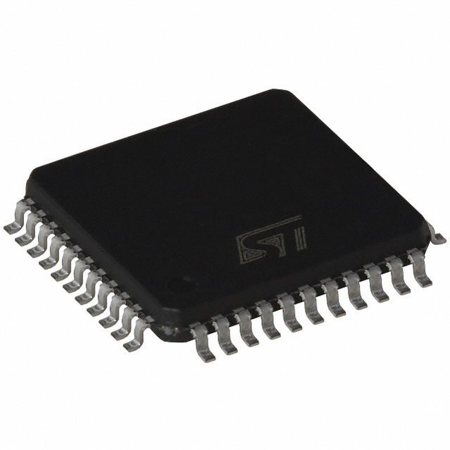
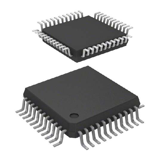
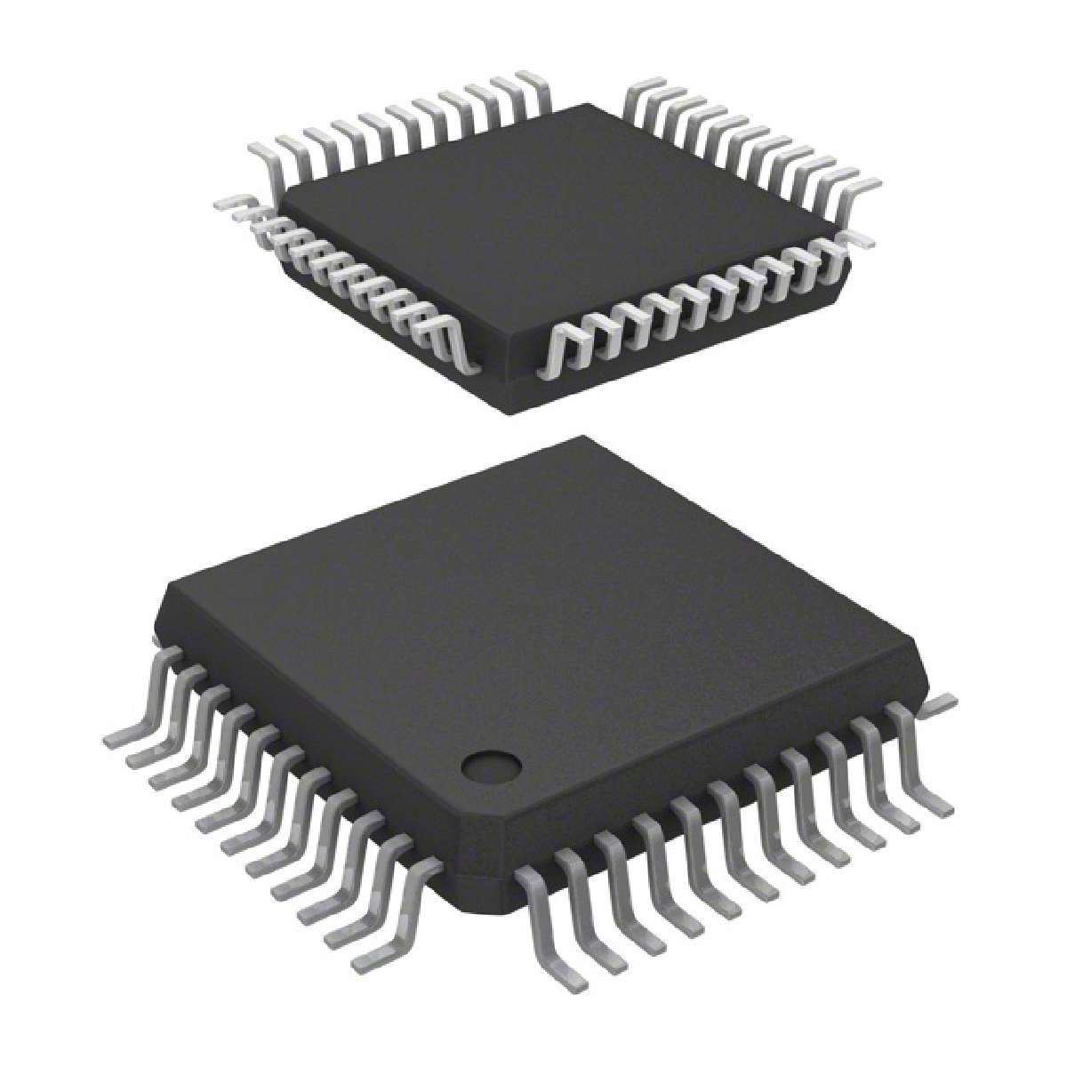
引脚数 44
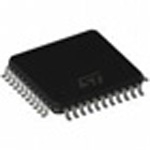
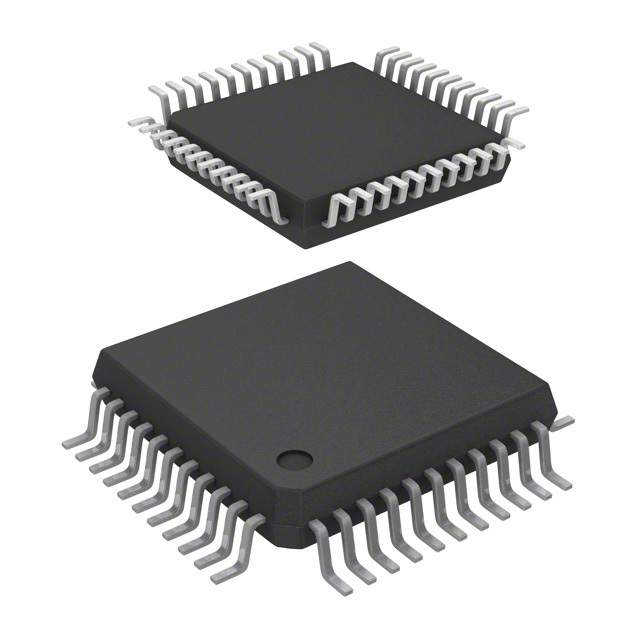
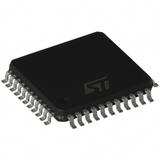
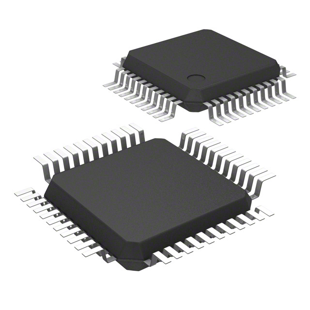
封装 LQFP-44
长度 10 mm
宽度 10 mm
高度 1.4 mm
封装 LQFP-44
工作温度 -40℃ ~ 85℃ TA
产品生命周期 Active
包装方式 Tray
RoHS标准 RoHS Compliant
含铅标准 Lead Free
ECCN代码 EAR99