


8位MCU的Flash或ROM存储器, ADC ,两个16位定时器, I2C , SPI , SCI INTERFACES 8-BIT MCU WITH FLASH OR ROM MEMORY, ADC, TWO 16-BIT TIMERS, I2C, SPI, SCI INTERFACES
INTRODUCTION
The ST72260Gx, ST72262Gx and ST72264Gx devices are members of the ST7 microcontroller family. They can be grouped as follows :
– ST72264Gx devices are designed for mid-range applications with ADC, I2C and SCI interface capabilities.
– ST72262Gx devices target the same range of applications but without I2C interface or SCI.
– ST72260Gx devices are for applications that do not need ADC, I2C peripherals or SCI.
All devices are based on a common industry standard 8-bit core, featuring an enhanced instruction set.
■ Memories
– 4 K or 8 Kbytes Program memory: ROM or Single voltage extended Flash XFlash with read-out protection write protection and In Circuit Programming and In-Application Programming ICP and IAP. 10K write/erase cycles guaranteed, data retention: 20 years at 55°C.
– 256 bytes RAM
■ Clock, Reset and Supply Management
– Enhanced reset system
– Enhanced low voltage supply supervisor LVD with 3 programmable levels and auxiliary voltage detector AVD with interrupt capability for implementing safe power-down procedures
– Clock sources: crystal/ceramic resonator oscillators, internal RC oscillator and bypass for external clock
– PLL for 2x frequency multiplication
– Clock-out capability
– 4 Power Saving Modes: Halt, Active Halt,Wait and Slow
■ Interrupt Management
– Nested interrupt controller
– 10 interrupt vectors plus TRAP and RESET
– 22 external interrupt lines on 2 vectors
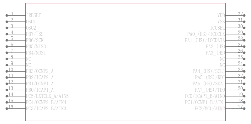
■ 22 I/O Ports
– 22 multifunctional bidirectional I/O lines
– 20 alternate function lines
– 8 high sink outputs
■ 4 Timers
– Main Clock Controller with Real time base and Clock-out capabilities
– Configurable watchdog timer
– Two 16-bit timers with: 2 input captures, 2 out put compares, external clock input on one timer, PWM and Pulse generator modes
■ 3 Communication Interfaces
– SPI synchronous serial interface
–I2C multimaster interface SMBus V1.1 Compliant
– SCI asynchronous serial interface
■ 1 Analog peripheral
– 10-bit ADC with 6 input channels
■ Instruction Set
– 8-bit data manipulation
– 63 basic instructionswith illegal opcode detection
– 17 main addressing modes
– 8 x 8 unsigned multiply instruction
■ Development Tools
– Full hardware/software development package
电源电压DC 5.00 V, 5.50 V max
时钟频率 8.00 MHz, 8.00 MHz max
RAM大小 256 x 8
I/O引脚数 22
存取时间 8.00 µs
模数转换数ADC 1
工作温度Max 85 ℃
工作温度Min -40 ℃
耗散功率Max 500 mW
电源电压Max 5.5 V
电源电压Min 2.7 V
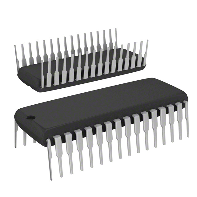
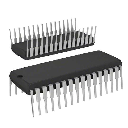
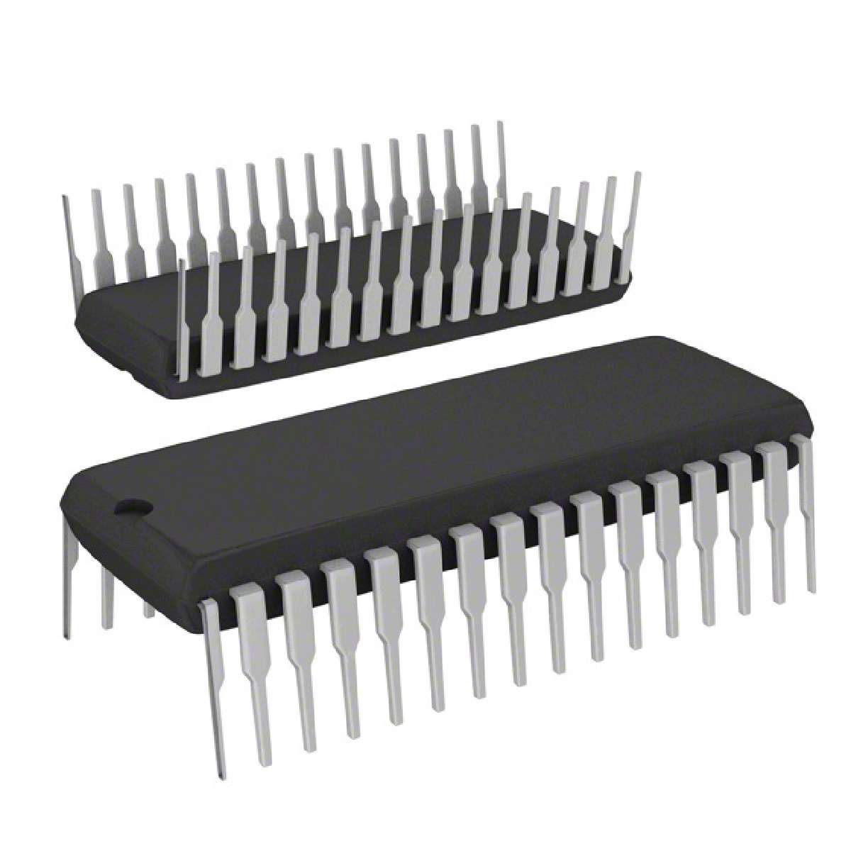
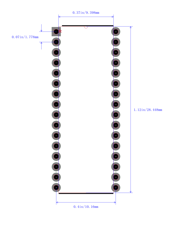
安装方式 Through Hole
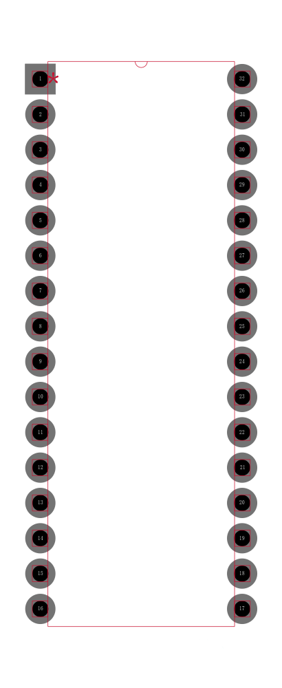
引脚数 32
封装 SDIP-32
长度 28.45 mm
宽度 8.89 mm
高度 3.56 mm
封装 SDIP-32
工作温度 -40℃ ~ 85℃
产品生命周期 Unknown
包装方式 Tube
RoHS标准 RoHS Compliant
含铅标准 Lead Free
| 型号/品牌 | 代替类型 | 替代型号对比 |
|---|---|---|
ST72F264G2B6 ST Microelectronics 意法半导体 | 当前型号 | 当前型号 |
ST72F264G1M6 意法半导体 | 类似代替 | ST72F264G2B6和ST72F264G1M6的区别 |
ST72F264G2M6 意法半导体 | 功能相似 | ST72F264G2B6和ST72F264G2M6的区别 |
ST72T251G1B6 意法半导体 | 功能相似 | ST72F264G2B6和ST72T251G1B6的区别 |