
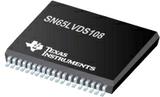


1:8 LVDS 时钟扇出缓冲器 38-TSSOP -40 to 85
DESCRIPON
The SN65LVDS108 is configured as one differential line receiver connected to eight differential line drivers. Individual output enables are provided for each output and an additional enable is provided for all outputs. The line receivers and line drivers implement the electrical characteristics of low-voltage differential signaling LVDS. LVDS, as specified in EIA/TIA-644, is a data signaling technique that offers low power, low noise emission, high noise immunity, and high switching speeds. Note: The ultimate rate and distance of data transfer is dependent upon the attenuation characteristics of the media, the noise coupling to the environment, and othersystem characteristics.
FEATURES
• One Line Receiver and Eight Line Drivers Configured as an 8-Port LVDS Repeater
• Line Receiver and Line Drivers Meet or Exceed the Requirements of ANSI EIA/TIA-644 Standard
• Typical Data Signaling Rates to 400 Mbps or Clock Frequencies to 400 MHz
• Enabling Logic Allows Individual Control of Each Driver Output, Plus All Outputs
• Low-Voltage Differential Signaling With Typical Output Voltage of 350 mV and a 100-Ω Load
• Electrically Compatible With LVDS, PECL, LVPECL, LVTTL, LVCMOS, GTL, BTL, CTT, SSTL, or HSTL Outputs With External Termination Networks
• Propagation Delay Times < 4.7 ns
• Output Skew Less Than 300 ps and Part-to-Part Skew Less Than 1.5 ns
• Total Power Dissipation at 200 MHz Typically Less Than 330 mW With 8 Channels Enabled
• Driver Outputs or Receiver Input Equals High Impedance When Disabled or With VCC < 1.5 V
• Bus-Pin ESD Protection Exceeds 12 kV
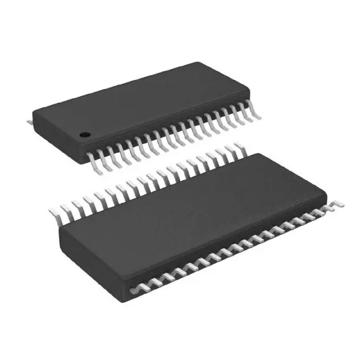
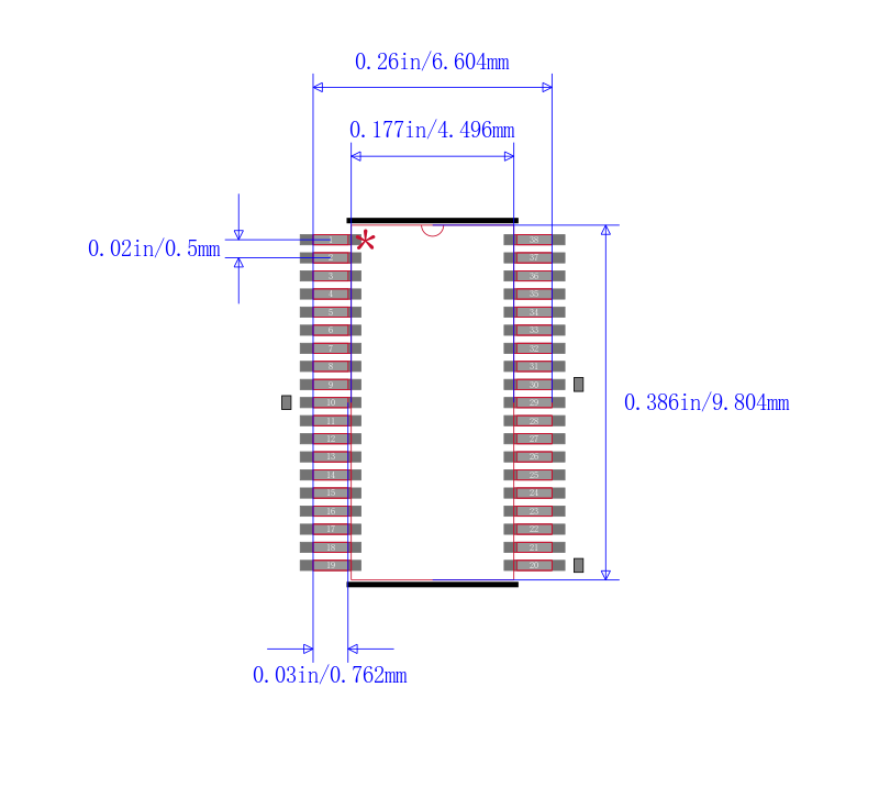
• Packaged in Thin Shrink Small-Outline Package With 20-Mil Terminal Pitch
频率 315 MHz
电源电压DC 3.30 V
输出接口数 8
供电电流 62 mA
耗散功率 1277 W
输入电容 5 pF
输入电流Min 20 μA
工作温度Max 85 ℃
工作温度Min -40 ℃
耗散功率Max 1277 mW
电源电压 3V ~ 3.6V
电源电压Max 3.6 V
电源电压Min 3 V
安装方式 Surface Mount
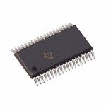
引脚数 38
封装 TSSOP-38
封装 TSSOP-38
工作温度 -40℃ ~ 85℃
产品生命周期 Active
包装方式 Tape & Reel TR
RoHS标准 RoHS Compliant
含铅标准 Lead Free


| 型号/品牌 | 代替类型 | 替代型号对比 |
|---|---|---|
SN65LVDS108DBTRG4 TI 德州仪器 | 当前型号 | 当前型号 |
SN65LVDS108DBT 德州仪器 | 类似代替 | SN65LVDS108DBTRG4和SN65LVDS108DBT的区别 |
SN65LVDS108DBTR 德州仪器 | 功能相似 | SN65LVDS108DBTRG4和SN65LVDS108DBTR的区别 |