
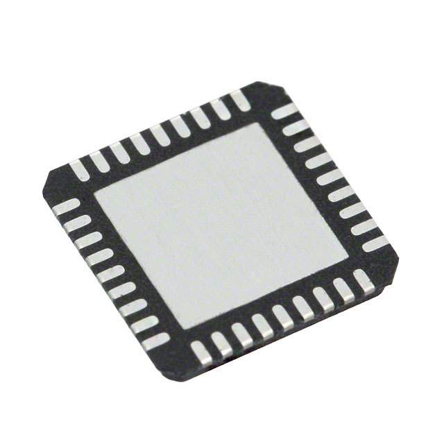
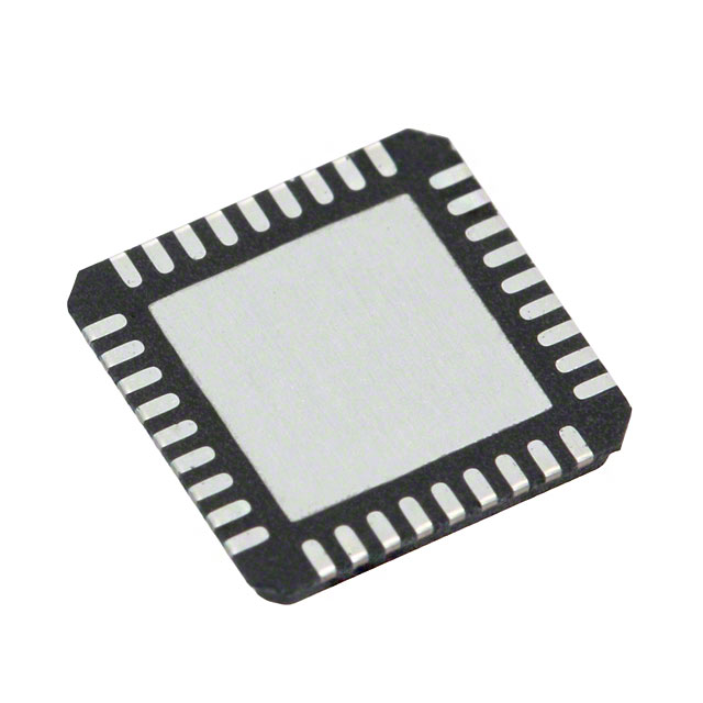
DSPLL 36Pin QFN
Description
The Si5325 is a low jitter, precision clock multiplier for applications requiring clock multiplication without jitter attenuation. The Si5325 accepts dual clock inputs ranging from 10 to 710 MHz and generates two clock outputs ranging from 10 to 945 MHz and select frequencies to 1.4 GHz. The
two outputs are divided down separately from a common source. The device provides virtually any frequency translation combination across this operating range.
Features
Generates any frequency from 10 to 945 MHz and select frequencies to 1.4 GHz from an input
frequency of 10 to 710 MHz
Low jitter clock outputs w/jitter generation as low as 0.6 ps rms 30 kHz–1.3 MHz
Integrated loop filter with selectable loop bandwidth 150 kHz to 2 MHz
Dual clock inputs w/manual or automatically controlled hitless switching
Dual clock outputs with selectable signal formatLVPECL, LVDS, CML, CMOS
Support for ITU G.709 and custom FEC ratios 255/238, 255/237, 255/236
LOS, FOS alarm outputs
Digitally-controlled output phase adjust
I2C or SPI programmable
On-chip voltage regulator for 1.8, 2.5, or 3.3 V ±10% operation
Small size: 6 x 6 mm 36-lead QFN
Pb-free, ROHS compliant
Applications
SONET/SDH OC-48/OC-192 line cards
GbE/10GbE, 1/2/4/8/10GFC line cards
ITU G.709 and custom FEC line cards
Optical modules
Wireless basestations
Data converter clocking
xDSL
SONET/SDH + PDH clock synthesis
Test and measurement
| 型号/品牌 | 代替类型 | 替代型号对比 |
|---|---|---|
SI5325C-B-GM Silicon Labs 芯科 | 当前型号 | 当前型号 |
SI5325C-C-GM 芯科 | 类似代替 | SI5325C-B-GM和SI5325C-C-GM的区别 |