


N 通道 JFET,ON Semiconductor### JFET 晶体管一系列 JFET(接线场效应晶体管)和 HEMT/HFET(高电子迁移率晶体管/异质结 FET)分立半导体设备。
N 通道 JFET,
### JFET
一系列 JFET(接线场效应晶体管)和 HEMT/HFET(高电子迁移率晶体管/异质结 FET)分立半导体设备。
得捷:
JFET N-CH 10MA 200MW CP
欧时:
### N 通道 JFET,ON Semiconductor### JFET 晶体管一系列 JFET(接线场效应晶体管)和 HEMT/HFET(高电子迁移率晶体管/异质结 FET)分立半导体设备。
e络盟:
晶体管, JFET, -30 V, 600 µA, 1.5 mA, -950 mV, SOT-23, JFET
艾睿:
If your circuit requires a high level of input resistance, this 2SK3666-2-TB-E JFET transistor from ON Semiconductor can provide you a solution. Its maximum power dissipation is 200 mW. This product will be shipped in tape and reel packaging so that components can be mounted effectively. It is made in a single configuration. This junction field effect transistor has an operating temperature range of -55 °C to 150 °C.
Allied Electronics:
2SK3666-2-TB-E N-channel JFET Transistor, 30 V, Idss 0.6 to 1.5mA, 3-Pin SOT-23
Chip1Stop:
Trans JFET N-CH 30V 10mA 3-Pin CP T/R
Verical:
Trans JFET N-CH 30V 10mA Si 3-Pin SC-59 T/R
罗切斯特:
Trans JFET N-CH 30V 10mA 3-Pin CP T/R
漏源极电阻 200 Ω
耗散功率 200 mW
漏源极电压Vds 30 V
输入电容Ciss 4pF @10VVds
额定功率Max 200 mW
工作温度Max 150 ℃
工作温度Min -55 ℃
耗散功率Max 200 mW
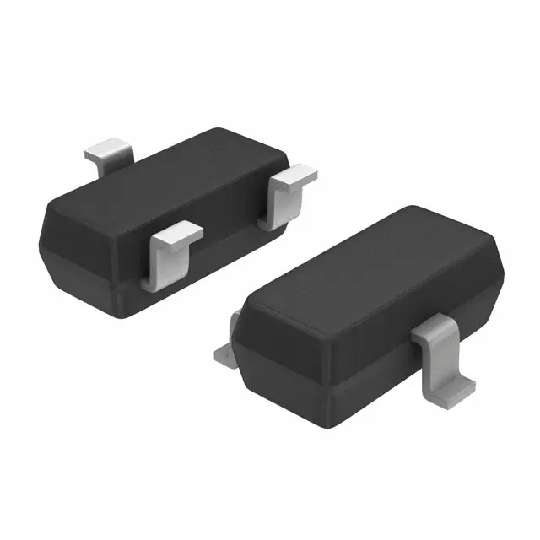
安装方式 Surface Mount
引脚数 3
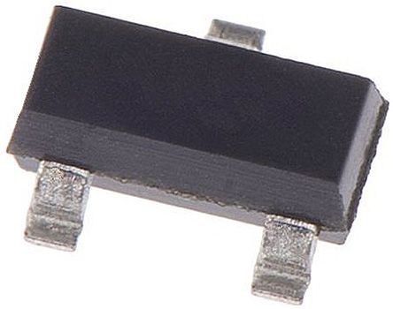
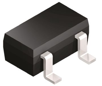
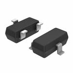
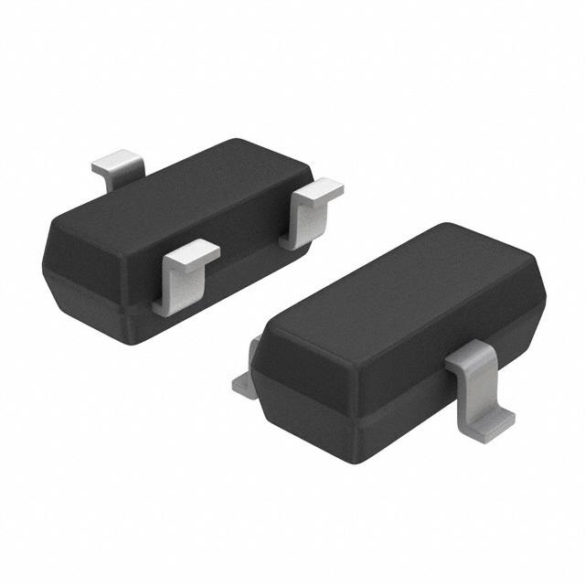
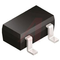
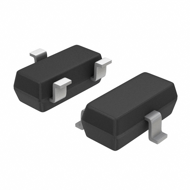
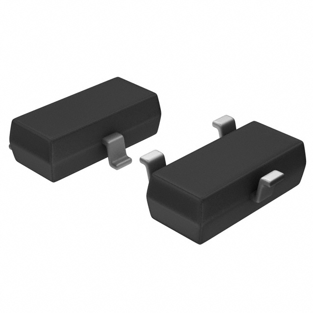
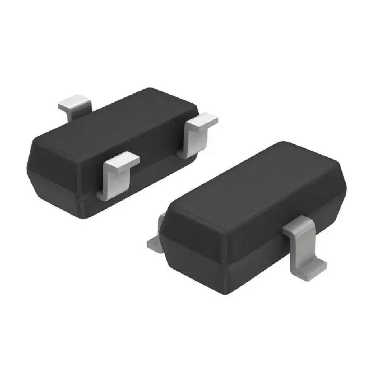
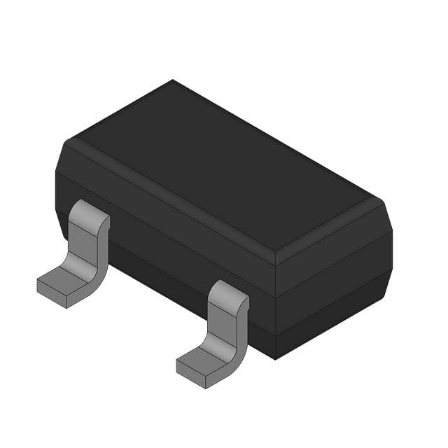
封装 SOT-23-3
长度 2.9 mm
宽度 1.5 mm
高度 1.1 mm
封装 SOT-23-3
材质 Silicon
工作温度 150℃ TJ
产品生命周期 Active
包装方式 Tape & Reel TR
制造应用 low-frequency,General-purpose Amplifier and Impedance converter
RoHS标准 RoHS Compliant
含铅标准 Lead Free
ECCN代码 EAR99