N 通道 JFET,ON Semiconductor### JFET 晶体管一系列 JFET(接线场效应晶体管)和 HEMT/HFET(高电子迁移率晶体管/异质结 FET)分立半导体设备。
N 通道 JFET,
### JFET
一系列 JFET(接线场效应晶体管)和 HEMT/HFET(高电子迁移率晶体管/异质结 FET)分立半导体设备。
得捷:
JFET N-CH 50MA 3CP
立创商城:
2SK2394-7-TB-E
欧时:
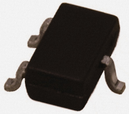
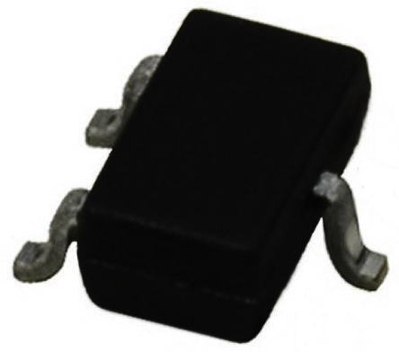
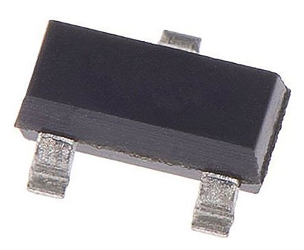
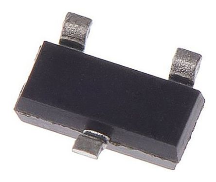
ON Semiconductor 2SK2394-7-TB-E N通道 JFET 晶体管, Vds=15 V, Idss: 16 → 32mA, 3引脚 CP封装
艾睿:
This 2SK2394-7-TB-E JFET from ON Semiconductor can be used as an electrical switch, amplifier, or voltage-controlled resistor by utilizing a diode-like structure. Its maximum power dissipation is 200 mW. This component will be shipped in tape and reel packaging to allow for effective mounting and safe delivery. It is made in a single configuration. This junction field effect transistor has a minimum operating temperature of -55 °C and a maximum of 150 °C.
Allied Electronics:
2SK2394-7-TB-E N-channel JFET Transistor; 15 V; Idss 16 - 32mA; 3-Pin CP
安富利:
* Large Forward Transfer Admittance * Small Ciss * Small-sized package permitting 2SK2394-applied sets to be made small slim * Ultralow noise figure
Chip1Stop:
Trans JFET N-CH 15V 50mA Si Automotive 3-Pin Case CP T/R
Verical:
Trans JFET N-CH 15V 50mA Si Automotive 3-Pin Case CP T/R
Win Source:
JFET N-CH 50MA 200MW CP
耗散功率 200 mW
漏源极电压Vds 15 V
输入电容Ciss 10pF @5VVds
额定功率Max 200 mW
工作温度Max 150 ℃
工作温度Min -55 ℃
耗散功率Max 200 mW
安装方式 Surface Mount
引脚数 3
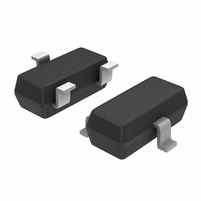
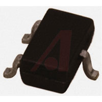
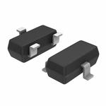
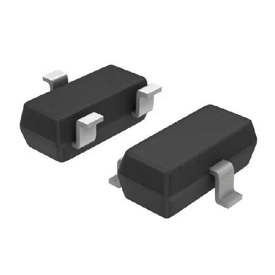
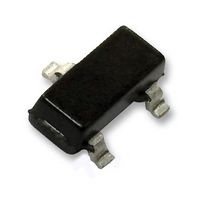
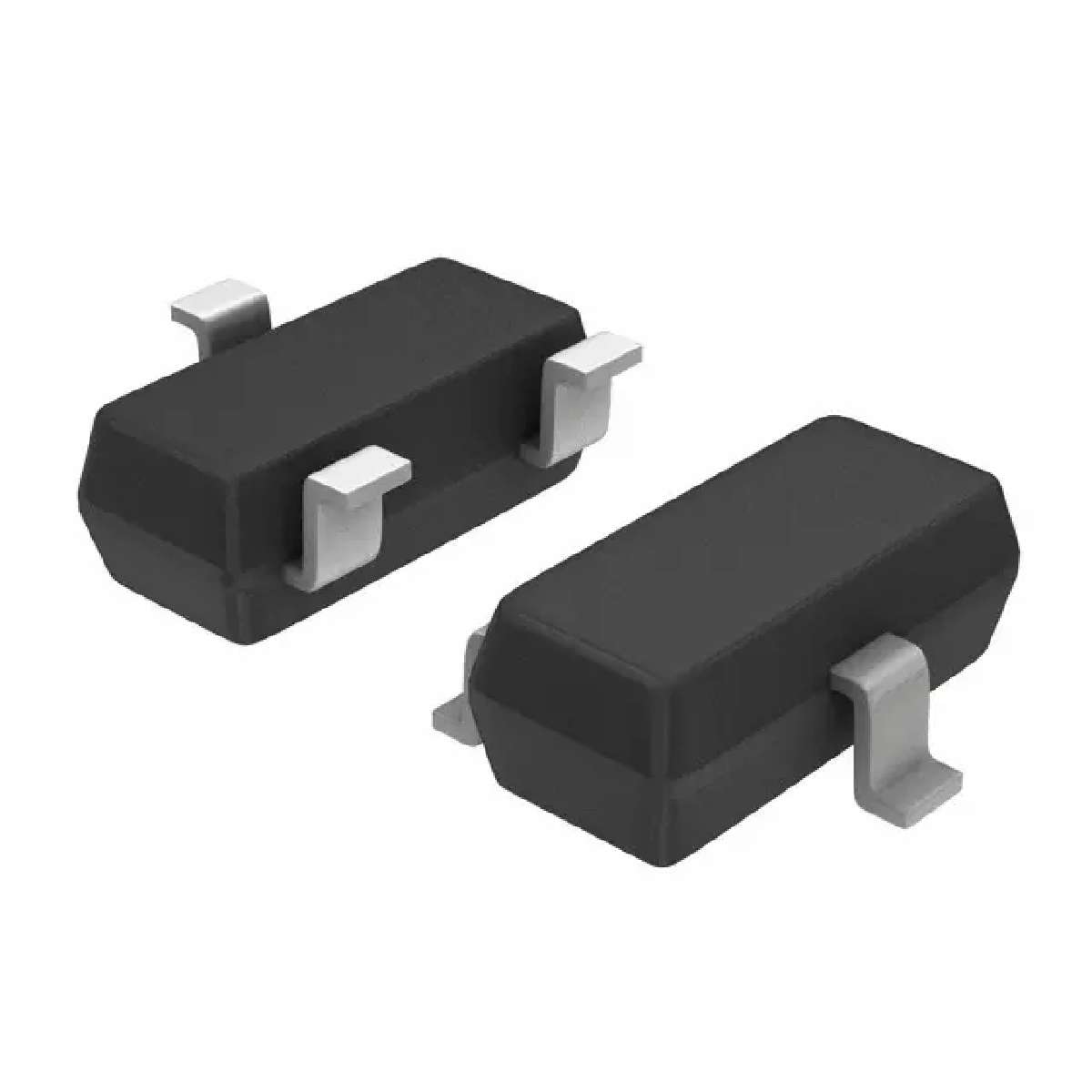
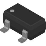
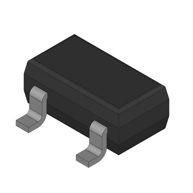
封装 SOT-23-3
长度 2.9 mm
宽度 1.5 mm
高度 1.1 mm
封装 SOT-23-3
材质 Silicon
工作温度 150℃ TJ
产品生命周期 Active
包装方式 Tape & Reel TR
制造应用 Low-noise amplifier, AM tuner RF amplifier
RoHS标准 RoHS Compliant
含铅标准 Lead Free
ECCN代码 EAR99
| 型号/品牌 | 代替类型 | 替代型号对比 |
|---|---|---|
2SK2394-7-TB-E ON Semiconductor 安森美 | 当前型号 | 当前型号 |