
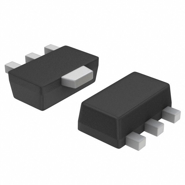

PNP 晶体管,超过 1A,ON Semiconductor### 标准带 S 或 NSV 前缀的制造商部件号具有汽车资格,符合 AEC-Q101 标准。### 双极性晶体管,On SemiconductorON Semiconductor 的各种双极晶体管,包括以下类别:小信号晶体管 功率晶体管 双晶体管 复合晶体管对 高电压晶体管 射频晶体管 双极/FET 晶体管
通用 PNP ,超过 1A,
### 标准
带 S 或 NSV 前缀的制造商部件号具有汽车资格,符合 AEC-Q101 标准。
得捷:
TRANS NPN 50V 4A PCP
立创商城:
2SC5566-TD-E
欧时:
ON Semiconductor 2SC5566-TD-E , NPN 晶体管, 4 A, Vce=50 V, HFE:200, 1 MHz, 3引脚 PCP封装
艾睿:
Implement this NPN 2SC5566-TD-E GP BJT from ON Semiconductor to add switching and amplifying capabilities to your electronic circuit design. This bipolar junction transistor&s;s maximum emitter base voltage is 6 V. Its maximum power dissipation is 1300 mW. This component will be shipped in tape and reel packaging to allow for effective mounting and safe delivery. It has a maximum collector emitter voltage of 100 V and a maximum emitter base voltage of 6 V. This bipolar junction transistor has an operating temperature range of -55 °C to 150 °C.
Allied Electronics:
ON Semi 2SC5566-TD-E NPN Bipolar Transistor; 4 A; 50 V; 3-Pin PCP
安富利:
Trans GP BJT NPN 100V 4A 4-Pin3+Tab PCP T/R
Verical:
Trans GP BJT NPN 100V 4A 1300mW 4-Pin3+Tab SOT-89 T/R
罗切斯特:
Trans GP BJT NPN 100V 4A 4-Pin3+Tab SOT-89 T/R
Win Source:
TRANS NPN 50V 4A SOT89-3
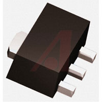
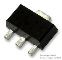
频率 400 MHz
针脚数 3
极性 N-Channel, NPN
耗散功率 1.3 W
击穿电压集电极-发射极 50 V
集电极最大允许电流 4A
最小电流放大倍数hFE 200 @500mA, 2V
最大电流放大倍数hFE 560
额定功率Max 1.3 W
直流电流增益hFE 200
工作温度Max 150 ℃
工作温度Min -55 ℃
耗散功率Max 1300 mW
安装方式 Surface Mount
引脚数 3
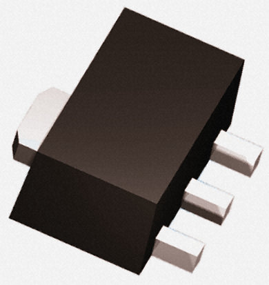
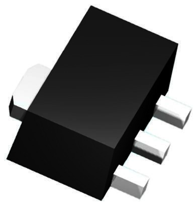
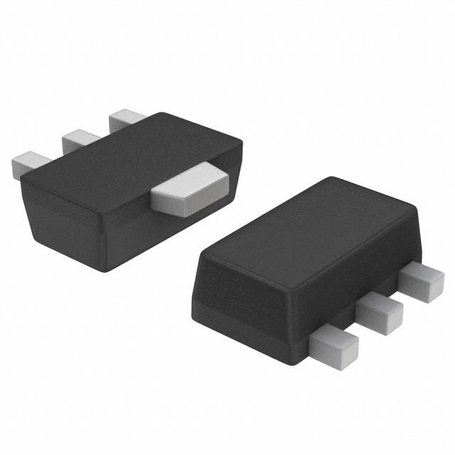
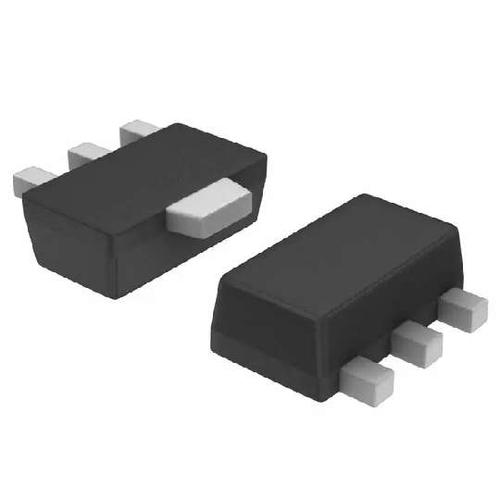
封装 TO-243
长度 4.5 mm
宽度 2.5 mm
高度 1.5 mm
封装 TO-243
工作温度 150℃ TJ
产品生命周期 Active
包装方式 Tape & Reel TR
RoHS标准 RoHS Compliant
含铅标准 Lead Free
ECCN代码 EAR99
| 型号/品牌 | 代替类型 | 替代型号对比 |
|---|---|---|
2SC5566-TD-E ON Semiconductor 安森美 | 当前型号 | 当前型号 |
SC55 三洋 | 功能相似 | 2SC5566-TD-E和SC55的区别 |