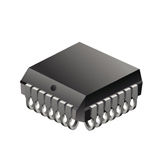
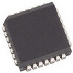


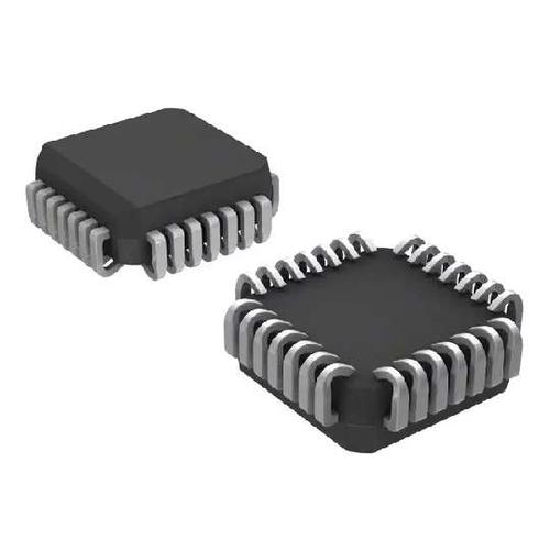
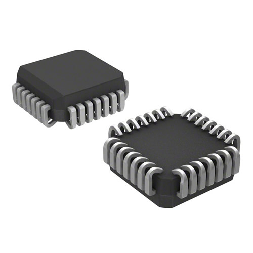
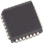
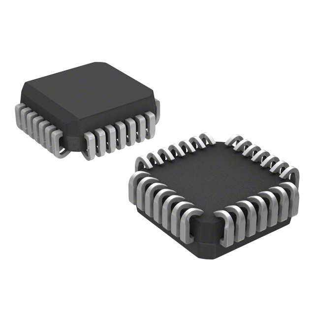
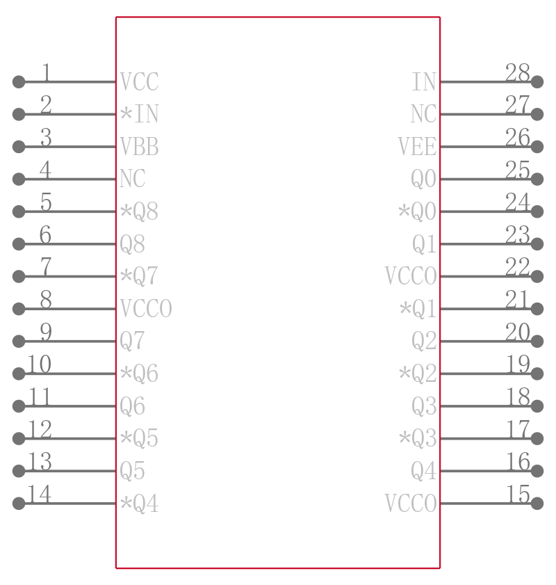
MC 系列 3.3 V 表面贴装 ECL 1:9 差分 时钟驱动器 - PLCC-28
The MC100LVE111 is a low skew 1-to-9 differential driver, designed with clock distribution in mind. The MC100LVE111"s function and performance are similar to the popular MC100E111, with the added feature of low voltage operation. It accepts one signal input, which can be either differential or single-ended if the V output is used. The signal is fanned out to 9 identical differential outputs. The LVE111 is specifically designed, modeled and produced with low skew as the key goal. Optimal design and layout serve to minimize gate to gate skew within a device, and empirical modeling is used to determine process control limits that ensure consistent tpd distributions from lot to lot. The net result is a dependable, guaranteed low skew device. To ensure that the tight skew specification is met it is necessary that both sides of the differential output are terminated into 50 W, even if only one side is being used. In most applications, all nine differential pairs will be used and therefore terminated. In the case where fewer than nine pairs are used, it is necessary to terminate at least the output pairs on the same package side as the pairs being used on that side, in order to maintain minimum skew. Failure to do this will result in small degradations of propagation delay on the order of 10-20 ps of the outputs being used which, while not being catastrophic to most designs, will mean a loss of skew margin. The MC100LVE111, as with most other ECL devices, can be operated from a positive V supply in PECL mode. This allows the LVE111 to be used for high performance clock distribution in +3.3 V systems. Designers can take advantage of the LVE111"s performance to distribute low skew clocks across the backplane or the board. In a PECL environment, series or Thevenin line terminations are typically used as they require no additional power supplies. For systems incorporating GTL, parallel termination offers the lowest power
Features
---
|
- .
- 200ps Part-to-Part Skew.
- .
- 50ps Output-to-Output Skew
- .
- ESD Protection: >2 KV HBM, >200 V MM
- .
- The 100 Series Contains Temperature Compensation
- .
- PECL Mode Operating Range: VCC= 3.0 V to 3.8 V with VEE = 0 V
- .
- NECL Mode Operating Range: VCC= 0 V with VEE= -3.0 V to -3.8 V
- .
- Internal Input Pulldown Resistors
- .
- Q Output will Default LOW with Inputs Open or at VEE
- .
- Meets or Exceeds JEDEC Spec EIA/JESD78 IC Latchup Test
- .
- Moisture Sensitivity Level 1 For Additional Information, see Application Note AND8003/D
- .
- Flammability Rating: UL-94 code V-0 @ 1/8", Oxygen Index 28 to 34
- .
- Transistor Count = 250 devices
- .
- Pb-Free Packages are Available
频率 1.50 GHz
电源电压DC 3.00V min
无卤素状态 Halogen Free
输出接口数 9
供电电流 55.0 mA
电路数 1
工作温度Max 85 ℃
工作温度Min -40 ℃
电源电压 3V ~ 3.8V
电源电压Max 3.8 V
电源电压Min 3 V
安装方式 Surface Mount
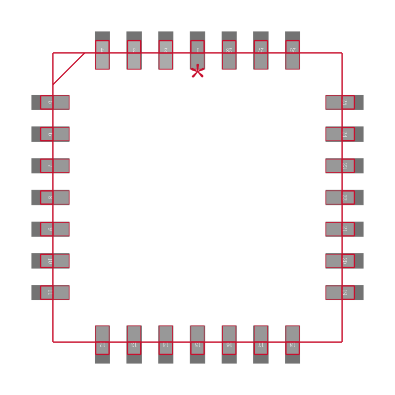
引脚数 28
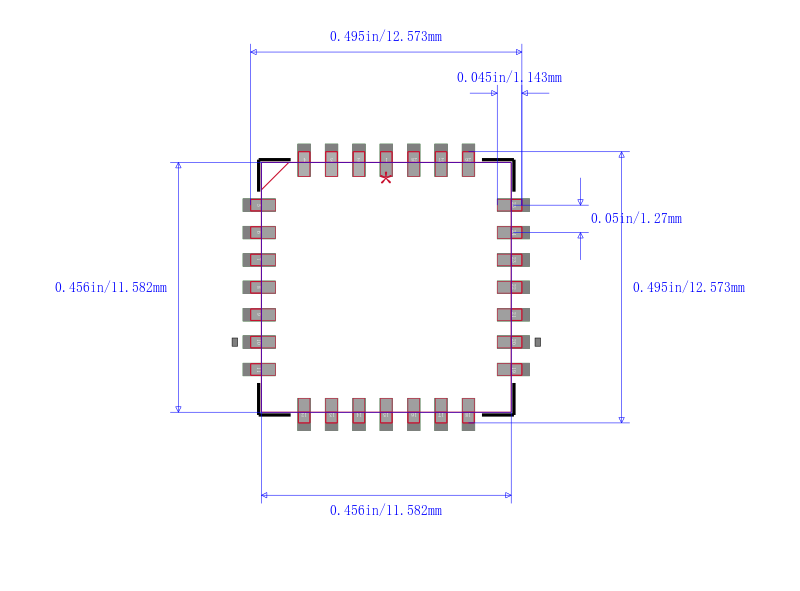
封装 PLCC-28
长度 11.58 mm
宽度 11.58 mm
高度 3.69 mm
封装 PLCC-28
工作温度 -40℃ ~ 85℃
产品生命周期 Active
包装方式 Tape & Reel TR
RoHS标准 RoHS Compliant
含铅标准 Lead Free
ECCN代码 EAR99
| 型号/品牌 | 代替类型 | 替代型号对比 |
|---|---|---|
MC100LVE111FNR2G ON Semiconductor 安森美 | 当前型号 | 当前型号 |
MC100LVE111FN 安森美 | 完全替代 | MC100LVE111FNR2G和MC100LVE111FN的区别 |
MC100E111FNG 安森美 | 类似代替 | MC100LVE111FNR2G和MC100E111FNG的区别 |
MC100LVE111FNG 安森美 | 类似代替 | MC100LVE111FNR2G和MC100LVE111FNG的区别 |