


模拟多路复用器/多路解复用器
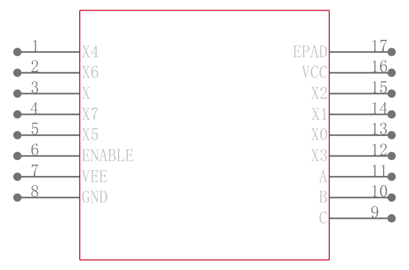
The MC74LVX4051 utilizes silicon-gate CMOS technology to achieve fast propagation delays, low ON resistances, and low leakage currents. This analog multiplexer/demultiplexer controls analog voltages that may vary across the complete power supply range from V The LVX4051 is similar in pinout to the LVX8051, HC4051A and the metal-gate MC14051B. The Channel-Select inputs determine which one of the Analog Inputs/Outputs is to be connected, by means of an analog switch, to the Common Output/Input. When the Enable pin is HIGH, all analog switches are turned off. The Channel-Select and Enable inputs are compatible with standard CMOS outputs. These inputs are over-voltage tolerant OVT forlevel translation from 6.0 V down to 3.0 V. This device has been designed so the ON resistance R is more linear over input voltage than R of metal-gate CMOS analog switches, and High-Speed CMOS analog switches.
Features
---
|
- .
- Fast Switching and Propagation Speeds
- .
- Low Crosstalk Between Switches
- .
- Analog Power Supply Range VCC \- VEE = -3.0 V to +3.0 V
- .
- Digital Control Power Supply Range VCC \- GND = 2.5 to 6.0 V
- .
- Improved Linearity and Lower ON Resistance Than Metal-Gate, HSL, or VHC Counterparts
- .
- Low Noise
- .
- Designed to Operate on a Single Supply with VEE = GND, or Using Split Supplies up to +/- 3.3 V
- .
- Break-Before-Make Circuitry
- .
- Pb-Free Packages are Available*