

8位微控制器有两个时钟加速的80C51的核心具有1KB 3伏字节可擦除闪存的8位A / D转换器 8-bit microcontrollers with two-clock accelerated 80C51 core 1 kB 3 V byte-erasable flash with 8-bit A/D converter
The is a 8-bit Microcontroller based on a high performance processor architecture that executes instructions in two to four clocks, six times the rate of standard 80C51 devices. The device features 1kB byte-erasable flash code memory organized into 256-byte sectors and 16-byte pages and single-byte erasing allows any bytes to be used as non-volatile data storage, 128-byte RAM data memory, Two 16-bit timer/counters, 23-bit system timer that can also be used as a RTC, four input multiplexed 8-bit A/D converter/single DAC output and one analog comparator with selectable reference.
- .
- High performance 80C51 CPU
- .
- In-application programming IAP-Lite
- .
- Serial flash in-circuit programming ICP
- .
- Watchdog timer with separate on-chip oscillator
- .
- Low voltage reset brownout detect
- .
- Idle mode
- .
- Active-LOW reset
- .
- Programmable port output configuration options
- .
- Port input pattern match detect
- .
- LED drive capability 20mA on all port pins
- .
- Controlled slew rate port outputs to reduce EMI
- .
- 4 Interrupt priority levels
- .
- 2 Keypad interrupt inputs
- .
- Second data pointer
- .
- External clock input
- .
- Clock output
- .
- Schmitt trigger port inputs
- .
- Emulation support
时钟频率 18.0 MHz
RAM大小 128 b
位数 8
FLASH内存容量 1 KB
内存容量 1000 B
工作温度Max 85 ℃
工作温度Min 40 ℃
电源电压Max 3.6 V
电源电压Min 2.4 V
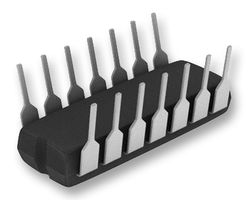
安装方式 Through Hole
引脚数 14
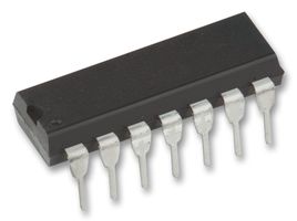
封装 PDIP-14
长度 19.5 mm
宽度 6.48 mm
高度 3.2 mm
封装 PDIP-14
产品生命周期 Unknown
包装方式 Each
制造应用 Industrial
RoHS标准 RoHS Compliant
REACH SVHC标准 No SVHC
REACH SVHC版本 2015/12/17