

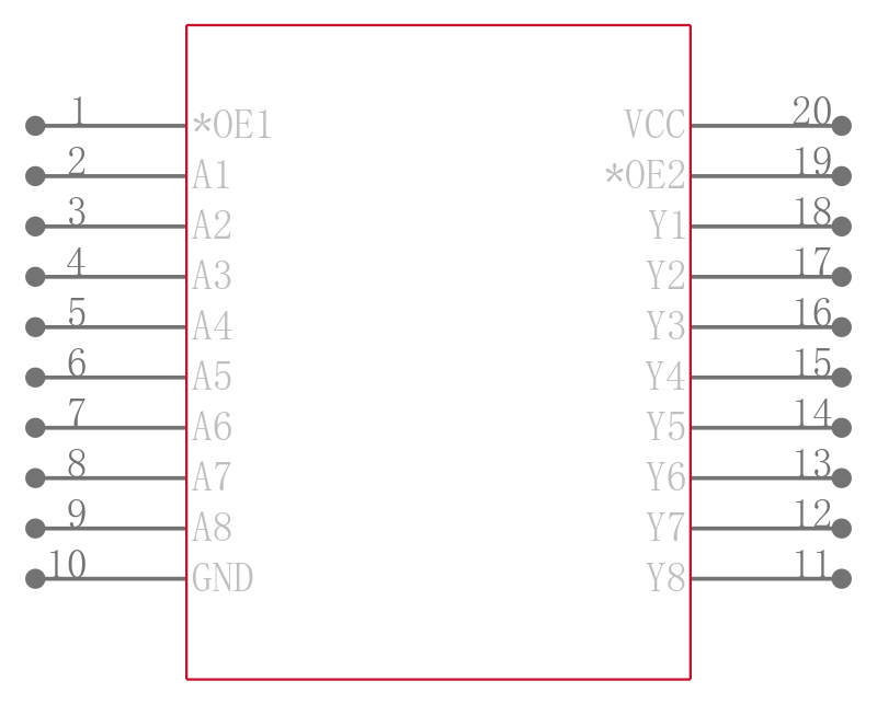
八路缓冲器/驱动器,具有三态输出 OCTAL BUFFER/DRIVER WITH 3-STATE OUTPUTS
DESCRIPON/ORDERING INFORMATION
The SN74LVC540A octal buffer/driver is designed for 2.7-V to 3.6-V VCC operation.
This device is ideal for driving bus lines or buffer-memory address registers. This device features inputs and outputs on opposite sides of the package that facilitate printed circuit board layout.
FEATURES
• Qualified for Automotive Applications
• ESD Protection Exceeds 2000 V Per
MIL-STD-883, Method 3015; Exceeds 200 V
Using Machine Model C = 200 pF, R = 0
• Operates From 2 V to 3.6 V
• Inputs Accept Voltages to 5.5 V
• Max tpd of 5.3 ns at 3.3 V
• Typical VOLP Output Ground Bounce < 0.8 V at VCC = 3.3 V, TA = 25°C
• Typical VOHV Output VOH Undershoot > 2 V at VCC = 3.3 V, TA = 25°C
• Supports Mixed-Mode Signal Operation on All Ports 5-V Input/Output Voltage With 3.3-V VCC
• Ioff Supports Partial-Power-Down Mode Operation
电源电压DC 2.00V ~ 3.60V
输出接口数 8
电路数 1
通道数 8
位数 8
传送延迟时间 5.30 ns
电压波节 3.30 V, 2.70 V
输出电流驱动 -1.00 mA
输入数 8
工作温度Max 125 ℃
工作温度Min -40 ℃
电源电压 2V ~ 3.6V
安装方式 Surface Mount
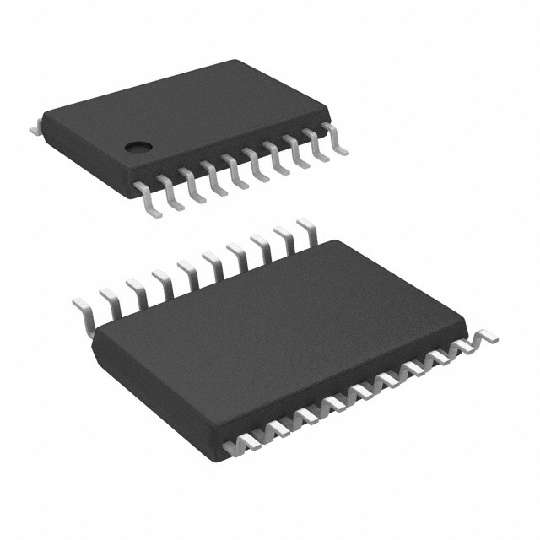
引脚数 20
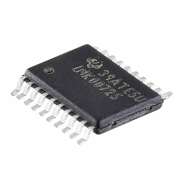
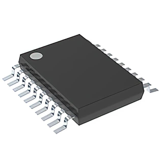
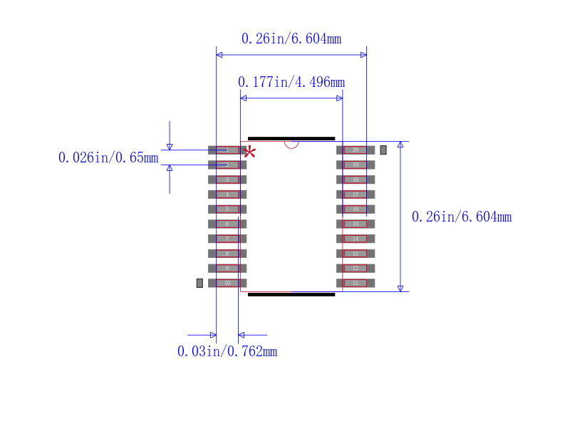
封装 TSSOP-20
长度 6.6 mm
宽度 4.5 mm
高度 1.05 mm
封装 TSSOP-20
工作温度 -40℃ ~ 125℃
产品生命周期 Active
包装方式 Tape & Reel TR
RoHS标准 RoHS Compliant
含铅标准 Lead Free

| 型号/品牌 | 代替类型 | 替代型号对比 |
|---|---|---|
SN74LVC540AQPWRQ1 TI 德州仪器 | 当前型号 | 当前型号 |
SN74LVC540AQPWREP 德州仪器 | 完全替代 | SN74LVC540AQPWRQ1和SN74LVC540AQPWREP的区别 |
SN74LVC540ADW 德州仪器 | 类似代替 | SN74LVC540AQPWRQ1和SN74LVC540ADW的区别 |
SN74LVC540APW 德州仪器 | 类似代替 | SN74LVC540AQPWRQ1和SN74LVC540APW的区别 |